
Microwave communication PCB is used in circuits where high frequency signals must move through the board with controlled loss, stable impedance, and reliable repeatability. These boards are often found in RF modules, antenna systems, wireless communication equipment, satellite communication devices, microwave links, and test platforms.
For this type of PCB, the material and manufacturing process are part of the electrical design. A small change in dielectric thickness, copper thickness, trace width, via structure, or connector launch can affect signal behavior. This is why microwave communication PCB projects should be reviewed before production, not only quoted from Gerber files.
For buyers, the main goal is not just to find a factory that can process high frequency material. The better goal is to work with a manufacturer that can review material, stackup, impedance, drilling, vias, surface finish, and batch consistency before fabrication starts.
Quick Summary
Microwave communication PCB is used in RF and microwave systems where signal transmission quality, impedance stability, and low-loss performance are required.
Common applications include microwave communication modules, antenna feed networks, wireless infrastructure, satellite communication equipment, RF front-end boards, and high frequency test devices.
The main review points include material selection, dielectric thickness, copper thickness, controlled impedance, connector launch design, via transitions, grounding, surface finish, and prototype-to-batch consistency.
Before quotation, buyers should provide Gerber files, drill files, stackup, material preference, working frequency, impedance requirement, board thickness, copper thickness, surface finish, quantity, and application background.
Where Microwave Communication PCBs Are Used
Microwave communication PCBs appear in many communication-related products where the board carries RF or microwave signals.
Typical applications include:
Microwave radio systems
Antenna feed circuits
RF front-end modules
Wireless infrastructure boards
Signal transmission modules
Point-to-point communication devices
Radar-related communication boards
High frequency test fixtures
Industrial RF communication equipment
Some boards are simple RF signal boards. Others combine microwave signal paths, control circuits, power sections, and connector interfaces in one layout. The manufacturing review should match the signal path, not only the board size or layer count.
A small two-layer board can still require careful impedance control if it carries a sensitive microwave path. A multilayer board may need hybrid materials if the design combines RF signals with digital or power sections.
Signal Path Risk Comes First
In microwave communication PCB projects, the RF signal path should be reviewed first.
The signal path may include:
Connector launch
Transmission line
Filter section
Antenna feed line
Via transition
Ground reference
Component pad transition
Output connector
Each transition can add reflection, loss, or discontinuity if it is not designed and manufactured correctly. The risk is not always visible from the top view of the PCB. A board can look clean but still perform poorly during RF testing.
Common signal path problems include poor connector transition, long via stubs, broken ground reference, inconsistent trace width, wrong dielectric thickness, and uncontrolled material substitution.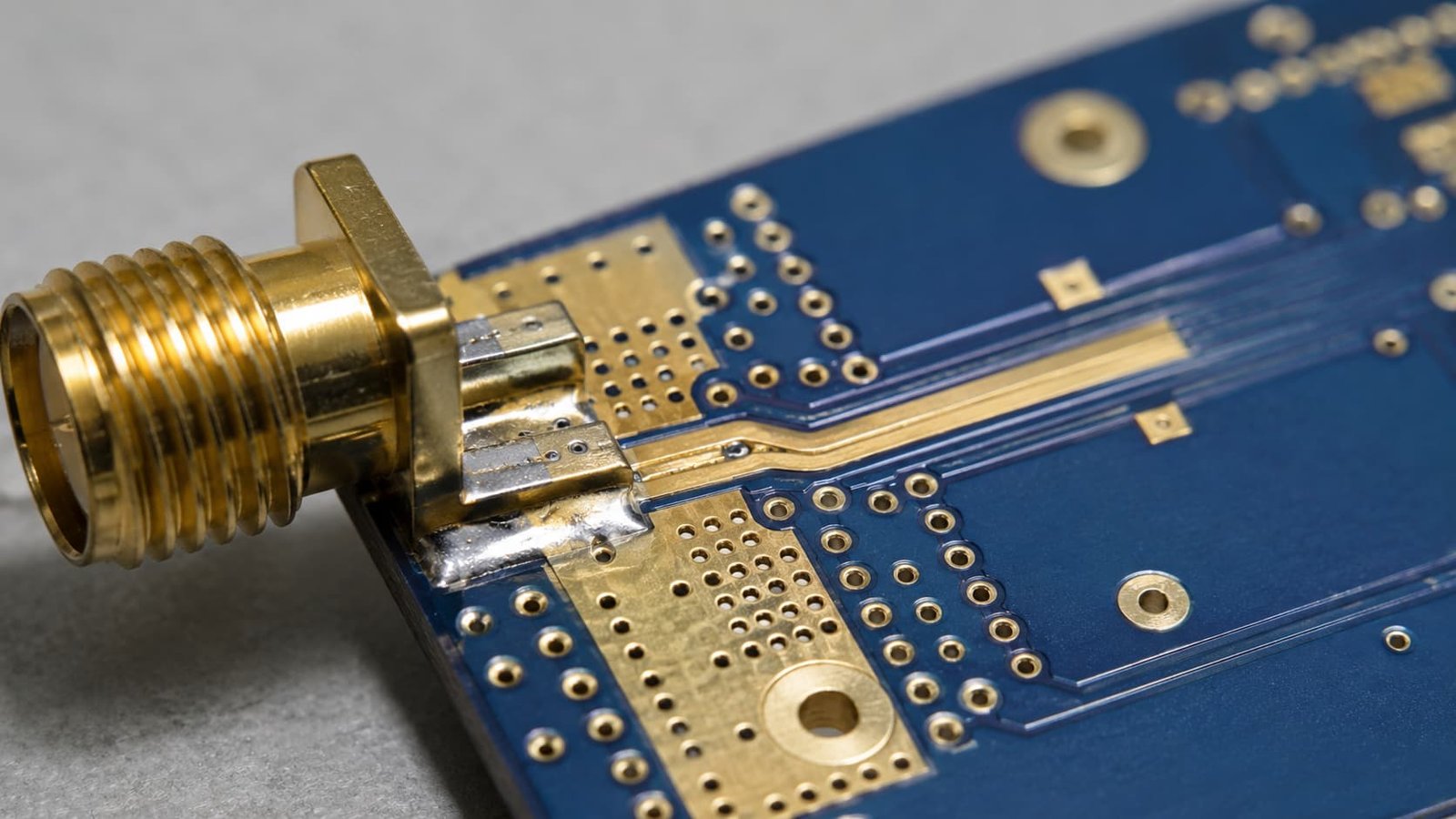
Material Selection
Material choice should be based on working frequency, loss target, stackup, and manufacturing feasibility.
Common material options for microwave communication PCB include:
PTFE laminates
Taconic materials
F4B materials
FR4 plus high frequency hybrid stackups
Other low-loss high frequency laminates
For less demanding RF sections, FR4 may sometimes be used. For microwave signal paths, low-loss materials are usually reviewed because standard FR4 may introduce higher loss and less stable dielectric behavior.
The material review should include:
Dk value
Df value
Dk tolerance
Dielectric thickness
Copper thickness
Copper roughness
Board thickness
Thermal and mechanical behavior
Material availability
Batch repeatability
A material should not be selected only because it is familiar. It should fit the actual signal requirement and production target.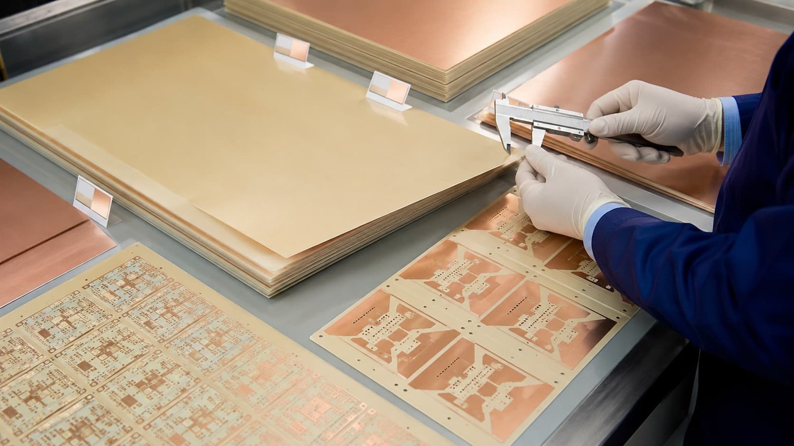
Stackup and Controlled Impedance
Stackup directly affects impedance and signal behavior.
Before production, the stackup should define:
Layer count
Material type
Dielectric thickness
Copper thickness
RF signal layer
Ground reference plane
Final board thickness
Surface finish
Controlled impedance target
Via structure
Controlled impedance is usually required for microwave transmission lines, antenna feed lines, connector areas, and RF signal paths. The impedance calculation should be based on the real production stackup, not only the early design assumption.
If the dielectric thickness or copper thickness changes during fabrication, the trace impedance may shift. At microwave frequencies, that shift can become visible in testing.
Connector Launch and Grounding
Connector launch design is one of the most common risk areas in microwave communication PCB.
Many boards use SMA, SMP, edge launch, board-to-board RF connectors, or custom RF interfaces. The transition from connector to PCB trace should be reviewed carefully.
The review should include:
Connector footprint
Pad size
Ground via placement
Trace transition
Reference plane continuity
Copper clearance
Mechanical strength
Assembly method
Surface finish
Grounding also needs close attention. A microwave signal needs a stable return path. If the ground plane is broken, too far away, or poorly connected with vias, the board may show reflection, radiation, or unstable test results.
Vias and Layer Transitions
Vias are often necessary in multilayer microwave communication PCB designs, but they can also create RF problems.
A via may work as a signal transition, ground connection, shielding structure, or part of a via fence. At microwave frequencies, via geometry and placement should not be treated as simple mechanical details.
The manufacturer should review:
Signal via size
Ground via spacing
Via stub length
Anti-pad clearance
Plated through-hole quality
Via fence layout
Connector grounding vias
Layer transition path
For microwave designs, via stubs and poor grounding can affect signal performance. If the board uses a multilayer stackup, via structure should be reviewed before fabrication starts.
Surface Finish Selection
Surface finish affects solderability, connector areas, assembly quality, storage, and sometimes RF-sensitive exposed areas.
Common options include:
ENIG
Immersion silver
OSP
Lead-free HASL
Hard gold for contact areas
Customer-specified finishes
ENIG is often used because it provides flatness and stable solderability. Immersion silver may be reviewed in some RF-sensitive designs. Hard gold may be needed for repeated contact or connector areas.
The finish should be selected according to RF requirement, assembly process, connector type, storage condition, and customer specification.
Manufacturing Review Before Production
Microwave communication PCB should not move into production without engineering review.
A practical review should include:
Material availability
Stackup feasibility
Controlled impedance requirement
Drilling tolerance
Plated through-hole reliability
Trace width tolerance
Copper thickness
Surface finish
Connector areas
Panelization
Inspection method
Prototype and batch plan
The manufacturer should check whether the requested material and stackup can be repeated in future orders. This is especially relevant for communication equipment that may move from prototype to batch production.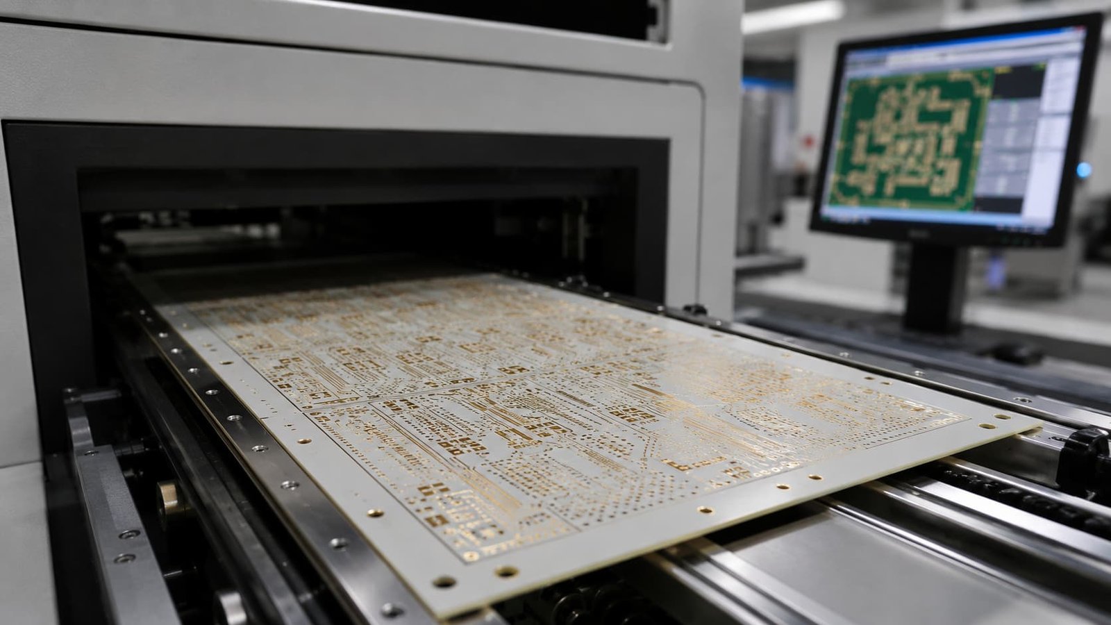
Procurement and Quotation Review
From a procurement point of view, microwave communication PCB should not be purchased only by comparing unit price.
The real cost includes material cost, fabrication difficulty, yield risk, impedance testing, inspection requirement, lead time, and repeatability. A lower material price may not save money if the board fails RF testing or needs several revisions.
Buyers should provide:
Gerber files
Drill files
Stackup
Material preference
Working frequency
Controlled impedance requirement
Board thickness
Copper thickness
Surface finish
Connector information
Quantity
Prototype or batch plan
Application background
If the material is not fixed, the working frequency and application background are very useful. They help the manufacturer suggest a practical material and stackup instead of making assumptions.
Common Mistakes to Avoid
Common mistakes include:
Choosing material only by price
Sending files without stackup
Missing working frequency
No controlled impedance information
Ignoring connector launch areas
Using too few ground vias
Changing material after layout
Ignoring via stubs
Selecting surface finish by habit
Not discussing batch repeatability
These problems often appear during RF testing, not visual inspection. A microwave communication PCB may look well manufactured but still fail if the signal path was not reviewed correctly.
Conclusion
Microwave communication PCB projects need careful review of material, stackup, controlled impedance, connector launch, vias, grounding, surface finish, and production repeatability.
For RF modules, microwave links, antenna systems, satellite communication devices, wireless infrastructure, and high frequency test platforms, the PCB is part of the signal path. It cannot be treated like a standard circuit carrier.
A reliable manufacturing process starts before production. Buyers should provide complete design files, frequency information, impedance requirements, material preferences, and application details so the PCB manufacturer can review the real production risk before fabrication begins.