RF PCB stackup design is one of the most important steps before manufacturing a high frequency circuit board. In RF, microwave, antenna, radar, wireless communication, and 5G PCB projects, the stackup directly affects controlled impedance, signal loss, grounding, isolation, board thickness, and final production consistency.
Unlike a standard low-frequency PCB, an RF PCB cannot be reviewed only by layer count and board thickness. The material type, dielectric thickness, copper thickness, reference plane, signal layer position, via structure, and lamination method can all affect electrical performance.
Before production, engineers and buyers should confirm the RF PCB stackup clearly with the manufacturer. This helps reduce impedance deviation, material mismatch, signal loss problems, drilling risks, and unexpected production changes.
Quick Summary
RF PCB stackup design should be reviewed before manufacturing because RF signals are sensitive to dielectric properties, trace geometry, copper thickness, and reference plane structure.
A good RF PCB stackup should define material type, layer count, dielectric thickness, copper thickness, signal layers, ground planes, controlled impedance targets, and final board thickness.
Common materials for RF PCB stackups include Rogers, PTFE, Taconic, F4B, and FR4 plus high frequency hybrid stackups.
For high frequency PCB projects, Riching PCB supports RF PCB manufacturing, microwave PCB manufacturing, high frequency PCB production, Rogers PCB materials, and RF Communication PCB manufacturing. Riching PCB’s RF communication page states that material selection, stackup design, dielectric thickness, copper thickness, impedance control, drilling quality, plated through-hole stability, and surface finish can directly affect signal performance and production consistency.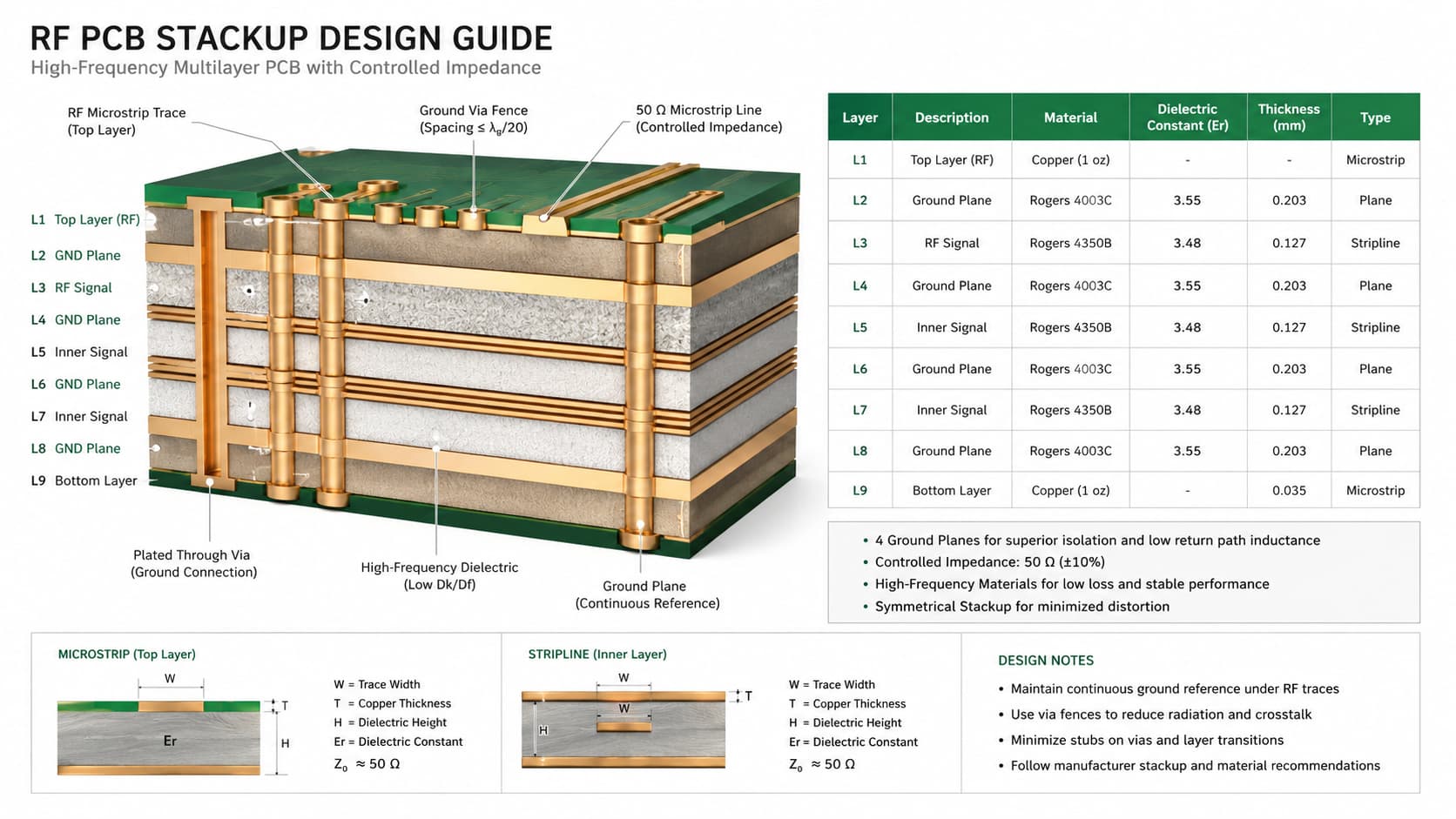
Why RF PCB Stackup Design Matters
In RF PCB design, copper traces work as transmission lines. Their performance depends on trace width, dielectric thickness, material Dk, copper thickness, and the nearby reference plane.
If the stackup is changed after the design is completed, the impedance may change. A small thickness adjustment, material substitution, or copper thickness change may affect signal reflection, insertion loss, antenna matching, or RF test results.
This is why RF PCB stackup should be confirmed before quotation and before manufacturing. The stackup is not only a mechanical structure. It is part of the electrical design.
Key Elements of an RF PCB Stackup
A complete RF PCB stackup should include:
Layer count
Material type
Dielectric thickness
Copper thickness
Signal layer position
Ground plane position
Power layer position
Controlled impedance target
Final board thickness
Surface finish
Via and drill structure
Lamination requirement
For RF and microwave PCB projects, the manufacturer should review whether the stackup can be produced reliably and whether the impedance target can be achieved with available materials and process tolerances.
Material Selection
Material selection is the foundation of RF PCB stackup design.
Standard FR4 may be suitable for some lower-frequency or less demanding RF applications, but RF and microwave circuits often require high frequency materials with more stable dielectric performance and lower signal loss.
Common RF PCB stackup materials include:
Rogers materials
PTFE laminates
Taconic materials
F4B materials
FR4 plus high frequency hybrid stackups
Rogers materials are commonly used in RF and microwave PCB projects. Riching PCB’s Rogers Materials page describes Rogers materials as suitable for RF, microwave, antenna, radar, satellite communication, and advanced communication PCB applications where stable dielectric performance, controlled impedance, low signal loss, and reliable high frequency transmission are important.
Rogers RO4000 LoPro fabrication guidelines also state that the guidelines are intended for processing double-sided and multilayer printed wiring boards using RO4000 LoPro laminates, which is relevant when evaluating high frequency stackup manufacturability.
Dielectric Thickness
Dielectric thickness is the distance between a signal trace and its reference plane. It has a direct effect on impedance.
For example, a microstrip RF trace on the outer layer depends on the dielectric thickness between the signal trace and the ground plane below it. If this thickness changes, the trace impedance changes.
Before production, the dielectric thickness should be confirmed based on:
Material datasheet
Available laminate thickness
Prepreg or bondply thickness
Copper thickness
Impedance target
Final board thickness
Manufacturing tolerance
For RF PCB projects, dielectric thickness should not be adjusted casually during production.
Copper Thickness
Copper thickness also affects impedance, conductor loss, current handling, and etching control.
In RF PCB manufacturing, both base copper and finished copper thickness should be reviewed. Plating can increase copper thickness, which may affect trace geometry and final impedance.
Copper thickness should be confirmed before impedance calculation. If the design assumes one copper thickness but production uses another, the finished PCB may not match the intended impedance.
For RF power circuits, thicker copper may be needed for current or thermal reasons. For fine RF traces, etching accuracy and finished trace width become important.
Ground Reference Plane
A stable ground reference plane is critical for RF PCB stackup design.
The ground plane provides a return path and helps create predictable transmission line behavior. If the ground plane is broken, poorly connected, or too far from the signal layer, RF performance may become unstable.
Analog Devices’ RF and mixed-signal PCB layout guidance notes that RF transmission lines should be kept apart where possible, crossing lines on separate layers should have a ground plane between them, and high-power signal lines should be kept away from other lines.
For RF PCB stackups, it is usually better to place a continuous ground plane close to important RF signal layers. Ground vias can also help provide stable return paths and reduce unwanted coupling.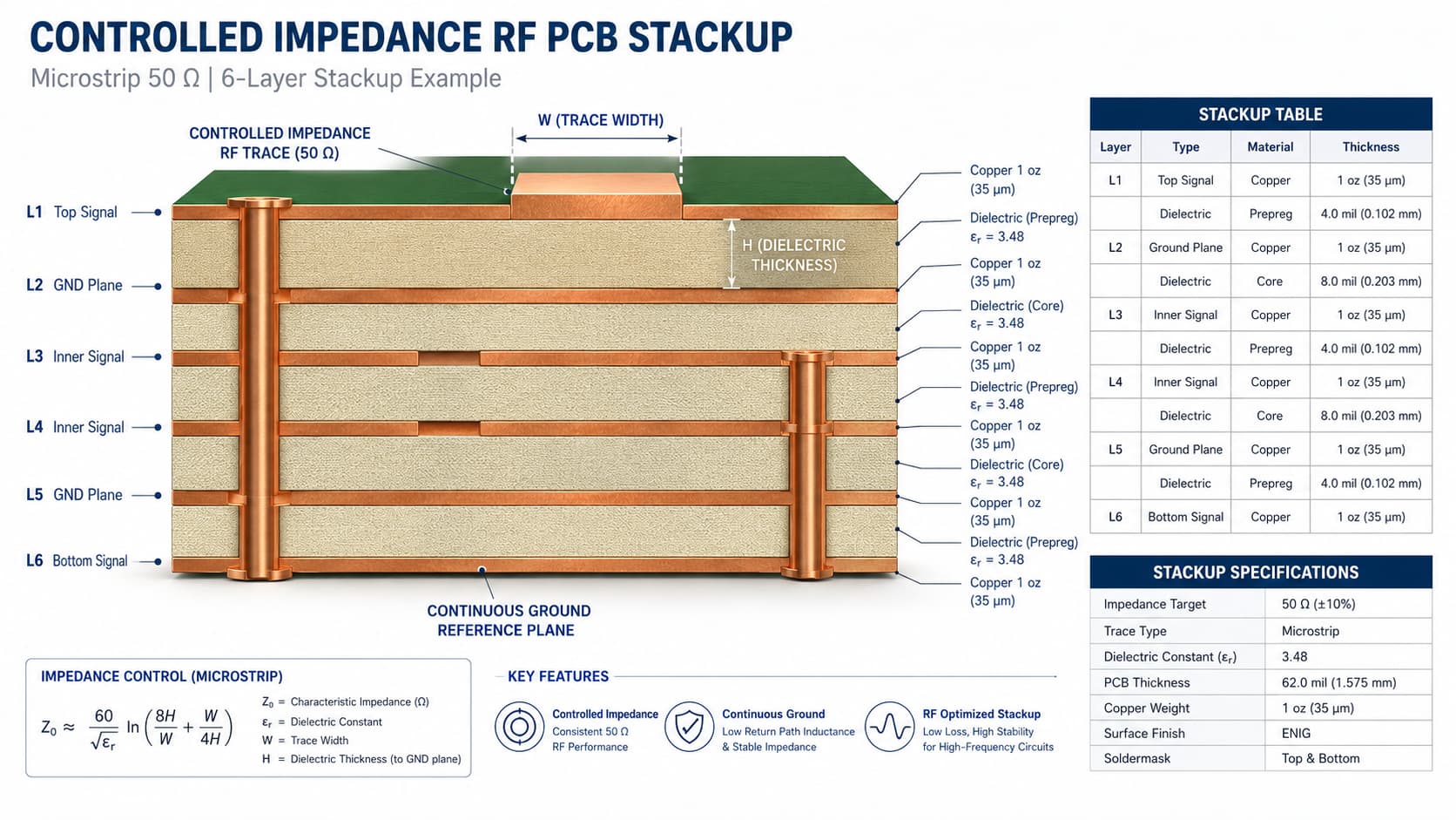
Signal Layer Position
RF signal layer placement should be planned based on impedance, shielding, routing length, component placement, and manufacturing feasibility.
Common RF transmission line structures include:
Microstrip
Stripline
Coplanar waveguide
Grounded coplanar waveguide
Controlled impedance feed line
Outer-layer microstrip is common because it is easy to route and inspect, but it may be affected by solder mask and the external environment. Inner-layer stripline can provide better shielding, but it requires multilayer structure and accurate lamination control.
The best option depends on application, frequency, impedance target, board size, material, and assembly requirement.
Controlled Impedance Review
Controlled impedance should be reviewed before manufacturing, not after fabrication.
Impedance is affected by:
Material Dk
Dielectric thickness
Trace width
Copper thickness
Reference plane distance
Solder mask
Etching tolerance
Plating thickness
If the customer provides an impedance table, the manufacturer should check whether the stackup supports the target impedance. If the stackup is not fixed, the manufacturer can help adjust dielectric thickness, trace width, or material choice.
Via Design in RF PCB Stackup
Vias can affect RF performance, especially near signal transitions, antenna feed lines, filters, connectors, and grounding structures.
Important via-related factors include:
Via size
Via position
Via stub length
Ground via placement
Plated through-hole quality
Signal transition structure
Layer transition path
For multilayer RF and microwave PCB projects, plated through-hole reliability should be reviewed together with material selection and stackup design. Riching PCB’s homepage lists stable plated through holes, tight tolerance drilling, multilayer lamination, controlled impedance, and engineering review before production as manufacturing capability areas for RF and microwave PCB projects.
Hybrid RF PCB Stackups
Some RF PCB projects use hybrid stackups that combine FR4 with high frequency materials.
A common example is using Rogers material on the RF signal layer while using FR4 for digital, power, or mechanical layers. This can help balance RF performance and cost.
However, hybrid stackups need careful review because different materials may have different thermal expansion, bonding behavior, and lamination characteristics.
Before choosing a hybrid RF PCB stackup, the manufacturer should review:
Material compatibility
Layer symmetry
Lamination process
Final board thickness
Controlled impedance
Drill and via reliability
Copper balance
Warpage risk
Surface Finish
Surface finish can affect solderability, assembly quality, bonding requirements, and sometimes RF performance.
Common surface finish options include immersion gold, immersion silver, OSP, HASL, and other customer-specified finishes.
For many RF and microwave PCB projects, immersion gold is commonly considered because it provides a flat surface and stable soldering performance. However, the final surface finish should be selected based on assembly method, application environment, RF performance requirement, and customer specification.
Stackup Review Before Quotation
To quote an RF PCB stackup accurately, the manufacturer usually needs:
Gerber files
Drill files
Full PCB stackup
Material requirement
Working frequency
Board thickness
Copper thickness
Controlled impedance table
Surface finish
Layer count
Quantity
Prototype or batch requirement
Application background
If the customer has not fixed the material or stackup, the manufacturer can review possible stackup options based on RF performance, cost target, and production feasibility.
Common Stackup Mistakes to Avoid
Common RF PCB stackup mistakes include:
Changing dielectric thickness after impedance calculation
Using material substitution without RF review
Breaking the ground reference plane under RF traces
Ignoring finished copper thickness
Using unclear stackup drawings
Not defining controlled impedance tolerance
Not reviewing hybrid material compatibility
Ignoring via transitions in RF paths
Choosing surface finish without assembly review
These problems may not be visible in the Gerber files, but they can affect RF performance and batch consistency.
Conclusion
RF PCB stackup design should be confirmed before manufacturing because high frequency performance depends on material selection, dielectric thickness, copper thickness, signal layer position, ground reference, impedance control, via design, and lamination feasibility.
For RF modules, microwave circuits, antenna boards, radar electronics, 5G devices, wireless infrastructure, and test equipment, stackup design is a key part of both electrical performance and manufacturing reliability.
Working with an experienced RF and high frequency PCB manufacturer can help reduce stackup risk, confirm material feasibility, improve impedance control, and support more stable production results.