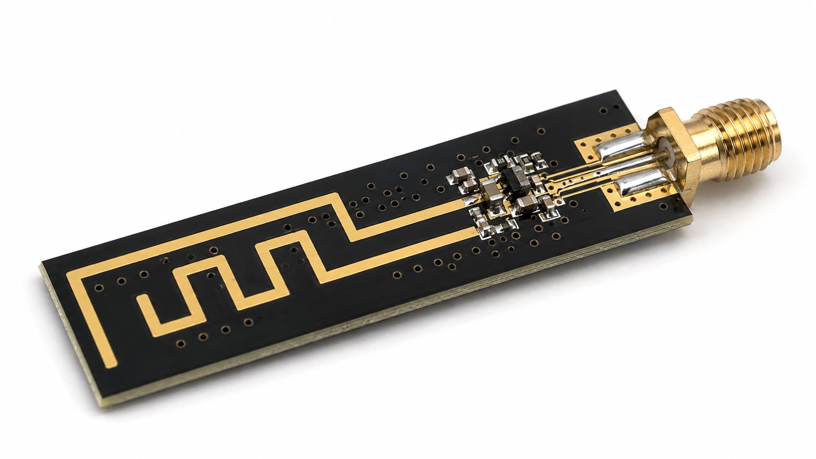
Antenna PCB is used in wireless devices and RF front-end modules because antenna performance depends on stable material properties, controlled impedance, accurate copper geometry, proper grounding, and reliable high frequency PCB manufacturing.
In many wireless products, the PCB is not only a support structure for components. The antenna trace, feed line, ground plane, dielectric layer, connector area, and RF matching circuit can all affect signal transmission, antenna efficiency, communication distance, and final product stability.
Compared with a standard FR4 control board, an antenna PCB for wireless devices may require high frequency materials, tighter copper control, impedance review, RF feed line optimization, and careful stackup design. For RF modules, wireless communication devices, IoT products, 5G equipment, radar sensors, and satellite communication systems, these factors can directly influence final RF performance.
Quick Summary
Antenna PCB for wireless devices is commonly used in RF modules, IoT devices, WiFi products, Bluetooth modules, GPS modules, RF front-end boards, antenna systems, communication equipment, and wireless infrastructure.
The most important antenna PCB requirements include controlled impedance, stable Dk and Df, low signal loss, accurate antenna trace geometry, reliable grounding, feed line control, and suitable material selection.
Common antenna PCB materials include Rogers, PTFE, Taconic, F4B, FR4, and FR4 plus high frequency hybrid stackups.
For antenna and RF communication projects, Riching PCB supports Antenna PCB manufacturing, RF PCB manufacturing, high frequency PCB production, microwave PCB manufacturing, and RF Communication PCB manufacturing for wireless devices, antenna modules, RF front-end circuits, and signal transmission boards. Riching PCB’s RF communication page describes support for high frequency PCB, RF PCB, microwave PCB, antenna PCB, and hybrid PCB manufacturing for RF modules and wireless devices.
Why Wireless Devices Need Antenna PCB
Wireless devices need antenna PCB structures to transmit and receive RF signals. These signals may be used for WiFi, Bluetooth, GPS, IoT communication, cellular modules, remote control systems, industrial wireless equipment, or RF sensing devices.
In a wireless product, antenna performance can be affected by the PCB material, copper trace shape, feed line impedance, ground plane, component placement, via structure, enclosure environment, and nearby metal parts. If these factors are not controlled, the device may show weak signal strength, poor range, unstable matching, or inconsistent test results.
Antenna PCB is commonly used in:
WiFi modules
Bluetooth devices
IoT wireless modules
GPS modules
RF front-end boards
Antenna matching circuits
5G communication devices
Industrial wireless equipment
Remote control systems
Wireless sensors
Test and measurement devices
For these applications, the PCB manufacturer should review material selection, stackup, impedance, copper thickness, antenna trace accuracy, drilling quality, surface finish, and production tolerance before manufacturing.
PCB Antenna vs External Antenna
Wireless products can use different antenna types, including PCB antennas, chip antennas, wire antennas, or external antennas. Texas Instruments’ antenna selection guide explains that PCB antennas, chip antennas, and wire antennas are commonly used for short-range RF devices, with size, cost, and performance being important selection factors.
A PCB antenna is created directly from the copper pattern on the circuit board. It can help reduce extra parts and simplify assembly, but it also makes the PCB material, layout, ground structure, and manufacturing tolerance more important.
An external antenna may provide more flexibility in some products, but it usually requires connectors, cables, mechanical space, and additional assembly considerations.
A chip antenna is compact and convenient, but it still depends on PCB layout, ground clearance, matching circuit design, and placement environment.
For many wireless devices, the right antenna structure depends on product size, frequency, performance target, mechanical design, and cost requirement.
Key Requirements for Antenna PCB
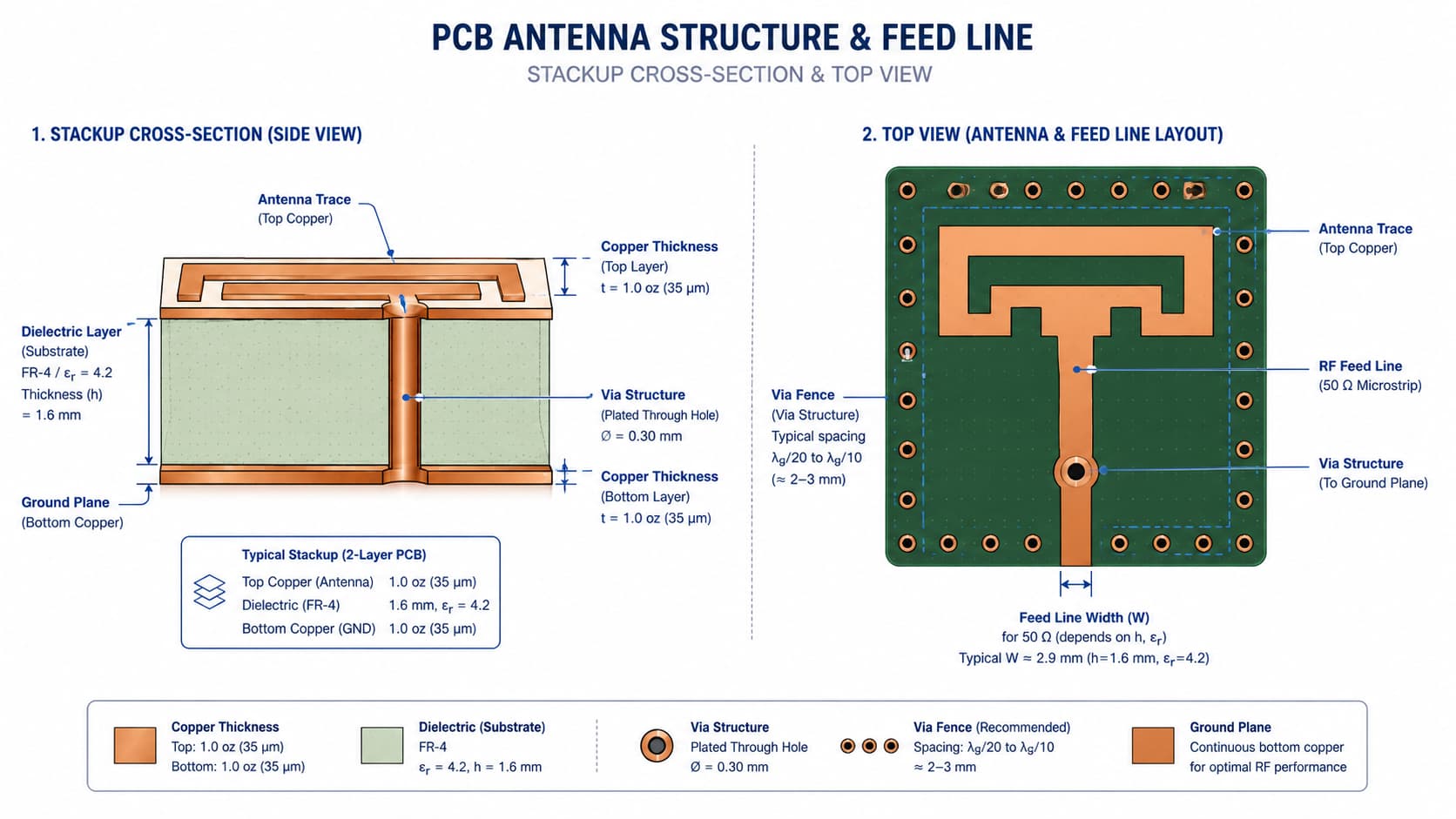
Controlled Impedance Feed Line
The antenna feed line connects the RF circuit to the antenna or RF connector. It is one of the most important areas in antenna PCB design.
Many RF systems use a 50-ohm feed line. If the feed line impedance is not controlled, signal reflection and mismatch may occur. This can reduce power transfer and affect antenna efficiency.
Infineon’s antenna design and RF layout guideline notes that the feed is generally 50 ohms in many low-power wireless RF PCB applications, although other impedance values may also be used depending on the design.
Controlled impedance depends on:
Material Dk
Dielectric thickness
Trace width
Copper thickness
Ground reference
Solder mask
Stackup design
Manufacturing tolerance
Stable Ground Plane
A stable ground plane is critical for antenna PCB performance.
The ground plane affects RF return paths, antenna tuning, feed line behavior, shielding, and signal stability. A broken or poorly connected ground plane may cause impedance instability, unwanted radiation, noise, or weak wireless performance.
For wireless devices, the PCB designer and manufacturer should pay attention to:
Ground plane continuity
Ground clearance near antenna area
Ground via placement
Shielding structure
RF return path
Antenna keep-out area
Connector grounding
Matching circuit grounding
For RF front-end modules, grounding becomes even more important because filters, amplifiers, switches, matching networks, and antenna feed structures are placed close together.
Material Stability
Antenna PCB material selection affects impedance, signal loss, antenna size, and frequency behavior.
Dielectric constant, also known as Dk, can affect signal speed, wavelength, antenna dimensions, and impedance. Dissipation factor, also known as Df, affects signal loss.
For lower-frequency and less demanding products, standard FR4 may be usable in some cases. For higher-frequency RF applications, microwave antennas, 5G modules, radar sensors, or satellite communication antenna boards, stable high frequency materials are often preferred.
Rogers states that its antenna-grade circuit laminates are engineered for high reliability, consistent performance, low circuit losses at high frequencies, and applications including antennas, feed networks, phased arrays, and radiating elements.
Material Options for Antenna PCB
Rogers Materials
Rogers materials are widely used in RF, microwave, antenna, radar, satellite communication, and wireless infrastructure applications.
For antenna PCB projects, Rogers materials may be selected when the design requires stable dielectric performance, low loss, controlled impedance, and reliable signal transmission. Rogers also offers antenna-grade laminates such as RO4700, which Rogers describes as an affordable alternative to conventional PTFE-based antenna materials for balancing cost and performance.
Riching PCB’s Rogers Materials page is a strong internal link here because it covers Rogers material support for RF, microwave, antenna, radar, satellite communication, 5G, wireless infrastructure, and test equipment applications.
PTFE Materials
PTFE materials are often used in low-loss RF and microwave antenna applications.
They may be suitable for antenna systems that require stable high-frequency performance, low signal loss, and reliable impedance behavior. PTFE can be considered for radar antenna boards, satellite communication antennas, microwave antennas, and advanced RF signal transmission structures.
However, PTFE PCB manufacturing is more difficult than standard FR4 processing. Drilling, plating, bonding, lamination, and dimensional control require experienced manufacturing capability.
Taconic Materials
Taconic materials can also be considered for RF and microwave antenna PCB projects.
They may be suitable when the project needs low dielectric loss, stable signal transmission, controlled impedance, and practical production feasibility. Riching PCB’s Taconic Materials page describes Taconic materials as suitable for RF modules, microwave communication, antenna systems, radar electronics, wireless infrastructure, and industrial high frequency applications.
F4B Materials
F4B materials may be considered for antenna PCB projects where performance, availability, and cost control need to be balanced.
For some RF antenna boards, communication modules, and wireless devices, F4B can provide better high frequency performance than standard FR4 while maintaining practical production efficiency.
However, F4B should still be reviewed based on working frequency, Dk, Df, impedance target, board thickness, and stackup feasibility.
FR4 + High Frequency Hybrid Stackups
Not every antenna PCB needs high frequency material across the entire board.
Some multilayer designs use high frequency material only on the antenna or RF layer, while using FR4 for supporting layers. This type of hybrid structure can help balance RF performance, mechanical strength, and production cost.
However, hybrid stackups require careful review because different materials may have different thermal expansion, bonding behavior, lamination behavior, and plated through-hole reliability.
Antenna PCB in RF Front-End Modules
RF front-end modules may include filters, switches, low-noise amplifiers, power amplifiers, matching circuits, connectors, and antenna feed structures.
In these modules, the antenna PCB area must support stable signal transmission between the RF components and the antenna. Poor feed line layout, weak ground reference, or inaccurate impedance may reduce module performance.
Important RF front-end PCB considerations include:
Short RF signal path
Controlled antenna feed line
Continuous ground reference
Stable matching circuit layout
Good shielding structure
Proper via placement
Copper thickness control
Surface finish selection
Thermal management
Connector footprint accuracy
Antenna Matching Circuit
Antenna matching circuits help match the antenna impedance with the RF system impedance.
If the antenna impedance is different from the RF transmission line, signal reflection may increase and less power may transfer to the antenna. Texas Instruments’ antenna basics matching material notes that transceivers and transmission lines are typically designed for 50 ohms, and impedance mismatch may require a matching circuit.
Antenna matching circuits may include inductors, capacitors, filters, or tuning components depending on the design. The PCB layout around these components should be carefully controlled because parasitic effects, trace length, pad geometry, and grounding can affect the final RF result.
Antenna Keep-Out Area
The antenna keep-out area is an important part of wireless device PCB design.
Copper, components, screws, batteries, metal housings, displays, cables, and shielding cans near the antenna may affect radiation performance. The keep-out area helps reduce unwanted interference around the antenna.
Before production, the antenna PCB design should review:
Antenna clearance
Nearby copper structures
Ground cutout area
Component distance
Enclosure material
Connector location
Battery or cable position
Mechanical installation environment
For custom antenna PCB projects, any mechanical or enclosure information can help the PCB manufacturer and RF engineer understand possible production risks.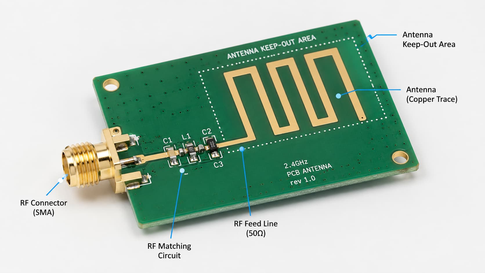
Antenna PCB Applications
Antenna PCB is used in many wireless and RF applications.
IoT Wireless Devices
IoT devices often require compact PCB antennas, RF modules, and stable wireless performance. The antenna PCB must balance size, cost, signal performance, and manufacturability.
For IoT devices, PCB antenna layout, ground plane design, matching circuit location, and enclosure impact should be reviewed carefully.
WiFi and Bluetooth Devices
WiFi and Bluetooth devices often use PCB antennas, chip antennas, or external antennas depending on size and performance requirements.
For these products, antenna feed line impedance, ground design, component placement, and matching circuit layout are important.
5G and Wireless Communication Modules
5G and wireless communication modules may require high frequency materials, low-loss signal paths, and controlled impedance structures.
For 5G antenna PCB or RF front-end modules, stackup design, material Dk, Df, copper accuracy, and surface finish should be reviewed before manufacturing.
Radar and Sensing Devices
Radar sensors and RF sensing devices may use antenna PCB structures for signal transmission and reception.
For radar antenna PCB, material loss, impedance matching, copper geometry, and manufacturing consistency are especially important.
Industrial RF Equipment
Industrial RF devices may be used in remote control systems, wireless monitoring equipment, factory automation, RF testing devices, and measurement systems.
For these applications, antenna PCB manufacturing should focus on signal stability, repeatability, reliability, and practical production control.
Manufacturing Requirements for Antenna PCB
Antenna PCB manufacturing requires careful control because small changes in copper geometry or material thickness may affect RF performance.
Important manufacturing requirements include:
Material verification
Stackup accuracy
Dielectric thickness control
Copper thickness control
Trace width accuracy
Etching tolerance
Controlled impedance production
Ground via quality
Plated through-hole reliability
Surface finish consistency
Dimensional stability
Final inspection
Engineering review before production
For antenna PCB projects, material substitution should not be made casually. Two materials with similar Dk may still perform differently because of Df, thickness tolerance, copper type, surface roughness, and processing behavior.
Surface Finish for Antenna PCB
Surface finish affects solderability, assembly reliability, and sometimes RF performance.
Common surface finish options may include immersion gold, immersion silver, OSP, HASL, or other customer-specified finishes.
For many antenna PCB and RF front-end PCB projects, immersion gold is often considered because it provides a flat surface and stable soldering performance. However, the final surface finish should depend on assembly method, RF requirement, product environment, and customer specification.
What Files Are Needed for Antenna PCB Quotation?
To quote an antenna PCB project accurately, the manufacturer usually needs complete engineering information.
Recommended files and details include:
Gerber files
Drill files
PCB stackup
Material requirement
Working frequency
Antenna type
Board thickness
Copper thickness
Surface finish
Controlled impedance requirement
Layer count
Quantity
Prototype or batch production requirement
Application background
Special tolerance or reliability requirements
If the antenna design is sensitive, it is also helpful to provide antenna location, keep-out requirement, matching circuit details, connector type, and mechanical environment.
How to Reduce Risk Before Antenna PCB Production
To reduce risk before antenna PCB manufacturing, engineers and buyers should confirm:
Working frequency is clear
Antenna type is confirmed
Material requirement is reviewed
Stackup is reviewed
Feed line impedance is defined
Ground plane design is checked
Antenna keep-out area is protected
Copper thickness is confirmed
Drill and via structures are reviewed
Surface finish is selected
Prototype and batch requirements are clear
Engineering review is completed before production
For antenna PCB and RF front-end module projects, early review can help reduce signal performance problems, production variation, and testing risk.
Conclusion
Antenna PCB plays an important role in wireless devices and RF front-end modules, including IoT products, WiFi modules, Bluetooth devices, 5G communication modules, radar sensors, industrial RF systems, and test equipment.
For antenna PCB projects, material selection, controlled impedance, feed line design, ground plane structure, antenna keep-out area, copper accuracy, via quality, stackup design, and surface finish all affect final wireless performance.
Rogers, PTFE, Taconic, F4B, FR4, and FR4 plus high frequency hybrid stackups can all be considered depending on working frequency, signal loss requirement, antenna structure, cost target, and manufacturing feasibility.
For custom antenna PCB projects, working with an experienced RF and high frequency PCB manufacturer can help reduce design risk, improve production consistency, and support more stable wireless signal performance.