These are approximate values calculated from standard microstrip formulas. Actual trace width must be confirmed with the fabricator using their production Dk from the material certificate. Solder mask over microstrip adds approximately 0.3–0.5 pF/cm of capacitance, which slightly reduces effective impedance — for designs requiring ±5% tolerance, request solder mask relief over RF traces or account for solder mask in the impedance calculation.
±10% vs ±5% Impedance Tolerance
Standard ±10% tolerance is appropriate for most commercial RF applications. Tighter ±5% tolerance requires additional TDR measurement points and extended manufacturing time, adding approximately 1 day to lead time. The cost difference is minimal — the lead time difference is the main consideration.
Important: ±5% tolerance must be specified explicitly on the fabrication drawing. Without a specified tolerance, the fabricator applies ±10% as default. Verbal confirmation is not sufficient — it must be on the drawing.
TDR Impedance Verification
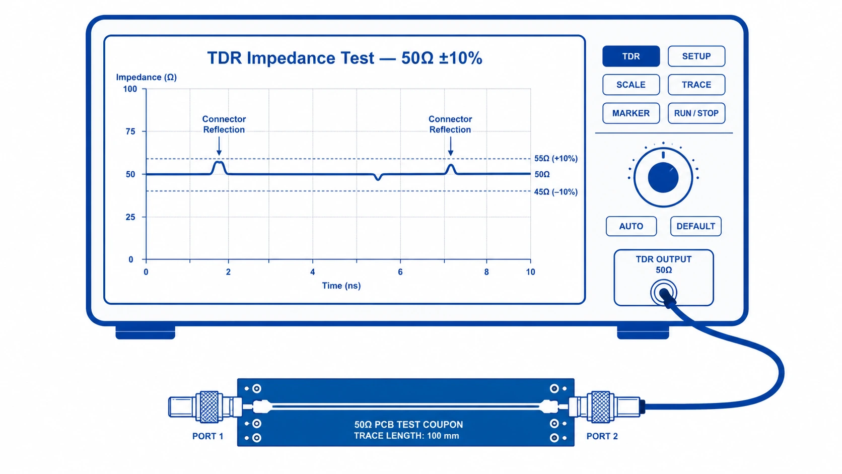
What TDR Measures
TDR (Time Domain Reflectometry) sends a fast-rise-time pulse down the transmission line and measures reflections. A perfectly matched 50Ω line produces no reflection. Impedance variations appear as positive (high impedance) or negative (low impedance) deflections on the TDR trace. The measurement gives impedance as a function of position along the line — identifying not just whether the board is in spec but where the variation occurs.
Test Coupon vs Production Trace
TDR is performed on test coupons — dedicated impedance test traces added to the production panel outside the board outline. Test coupons are manufactured under the same process conditions as the production board. For ±10% standard tolerance, one coupon per panel edge is standard. For ±5% tolerance or phased array applications, request multiple coupon locations across the panel to verify Dk uniformity.
Every Lot vs First Article
TDR on first article only means the fabricator verifies one prototype lot and assumes subsequent production lots match. For Rogers PCB, this is inadequate — Rogers material Dk varies between lots, and production process variations (etch variation, plating thickness) affect impedance. Riching PCB performs TDR on every production lot as standard. For phased array PCB and mmWave applications, request panel-level TDR verification at multiple locations.
What to Put on the Fabrication Drawing
Controlled impedance specification on the fabrication drawing should include:
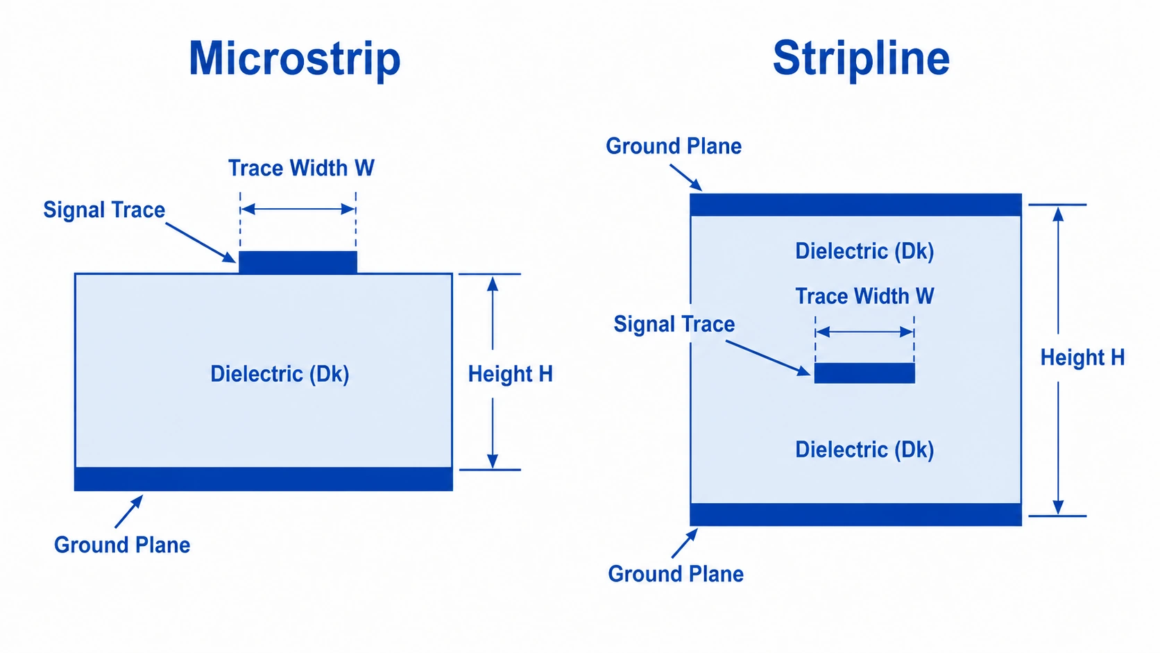
- Impedance structure type: microstrip, stripline, coplanar waveguide, differential pair
- Target impedance value: e.g. 50Ω single-ended, 100Ω differential
- Tolerance: ±10% or ±5%
- Reference layer: e.g. ’50Ω microstrip on L1 referenced to L2 ground plane’
- Material grade and dielectric thickness: e.g. ‘RO4350B 0.254 mm core’
- Copper weight: e.g. ‘1 oz finished copper on L1’
- TDR verification required: yes/no, and whether panel-level verification is needed
Missing any of these items forces the fabricator to make assumptions — which means the finished board may not match your design intent. Providing a complete impedance specification upfront eliminates this risk.
Common Controlled Impedance Mistakes
Using Nominal Dk Instead of Production Dk
Calculated trace width from Rogers RO4350B datasheet Dk 3.48 may be 0.56 mm. If the fabricator’s material lot measures Dk 3.53, the same 0.56 mm trace produces impedance of approximately 49.1Ω — within ±10% but potentially outside ±5%. Always request the material lot Dk certificate and recalculate.
Not Specifying Tolerance
Without a specified tolerance on the drawing, the fabricator applies ±10% default. If your design requires ±5%, this must be explicitly stated. There is no cost difference — only a lead time difference of approximately 1 day.
Specifying ±5% for Applications That Don’t Need It
±5% tolerance adds manufacturing complexity and approximately 1 day to lead time. For WiFi, Bluetooth, 5G sub-6GHz, and most commercial RF applications, ±10% is adequate. Reserve ±5% for phased array designs, mmWave applications above 20 GHz, and designs where insertion loss budget is tight.
Solder Mask Over RF Traces
Solder mask over microstrip RF traces adds capacitance loading that reduces effective impedance by 1–3Ω depending on mask thickness and Dk. For ±10% tolerance this is usually within budget. For ±5%, either request solder mask relief (LSOG) over RF traces or account for solder mask in the impedance calculation.
Controlled Impedance Capability at Riching PCB
- Standard tolerance: ±10%, TDR on every production lot
- Tight tolerance: ±5%, available on request — add approximately 1 day to lead time
- Panel-level TDR: available for phased array and mmWave applications
- Materials: RO4350B, RO4003C, RO3003, RT5880, Taconic, F4B — all in stock
- Material lot Dk certificate: available on request for every order
- line width: 2.5 mil — confirm for tight trace designs
Conclusion
Controlled impedance RF PCB requires confirmed production Dk (not nominal datasheet values), explicitly specified tolerance on the fabrication drawing, and TDR verification on every production lot. ±10% is standard for most RF applications; ±5% is required for phased array and mmWave designs above 20 GHz. For panel-level Dk uniformity verification, request multiple TDR coupon locations. Riching PCB performs TDR on every lot, provides material Dk certificates on request, and supports ±5% tolerance with panel-level verification. See high frequency PCB capabilities for full specifications, or Rogers materials overview for material Dk and thickness options.