F4B PCB materials are often considered when a project needs better high frequency performance than standard FR4, but the budget or application does not require premium RF laminates across the whole board.
That is the practical position of F4B in many RF and microwave PCB projects. It is not always the highest-performance choice, and it should not be treated as a direct replacement for every Rogers, PTFE, Taconic, or RT/duroid design. But for some RF modules, antenna boards, wireless communication circuits, industrial RF equipment, and cost-sensitive microwave projects, F4B can be worth reviewing.
For buyers, the decision should not start with “Is F4B cheap?” A better question is: can F4B meet the frequency, signal loss, impedance, stackup, and reliability requirements of this specific design?
Riching PCB supports F4B materials, RF PCB manufacturing, microwave PCB manufacturing, high frequency PCB manufacturing, and antenna PCB manufacturing for projects where material choice needs to balance performance, availability, and production cost.
Quick Summary
F4B materials can be considered for RF and microwave PCB projects where standard FR4 is not enough, but the project still needs cost control.
Typical applications include RF communication boards, antenna PCBs, wireless modules, industrial RF devices, microwave signal boards, and some high frequency test or control applications.
F4B should be reviewed based on working frequency, Dk, Df, board thickness, copper thickness, controlled impedance, surface finish, and stackup feasibility.
For higher-performance comparison, buyers often benchmark F4B against established RF laminate families such as Rogers RO4000 series laminates or AGC RF/Microwave laminates before making a final decision.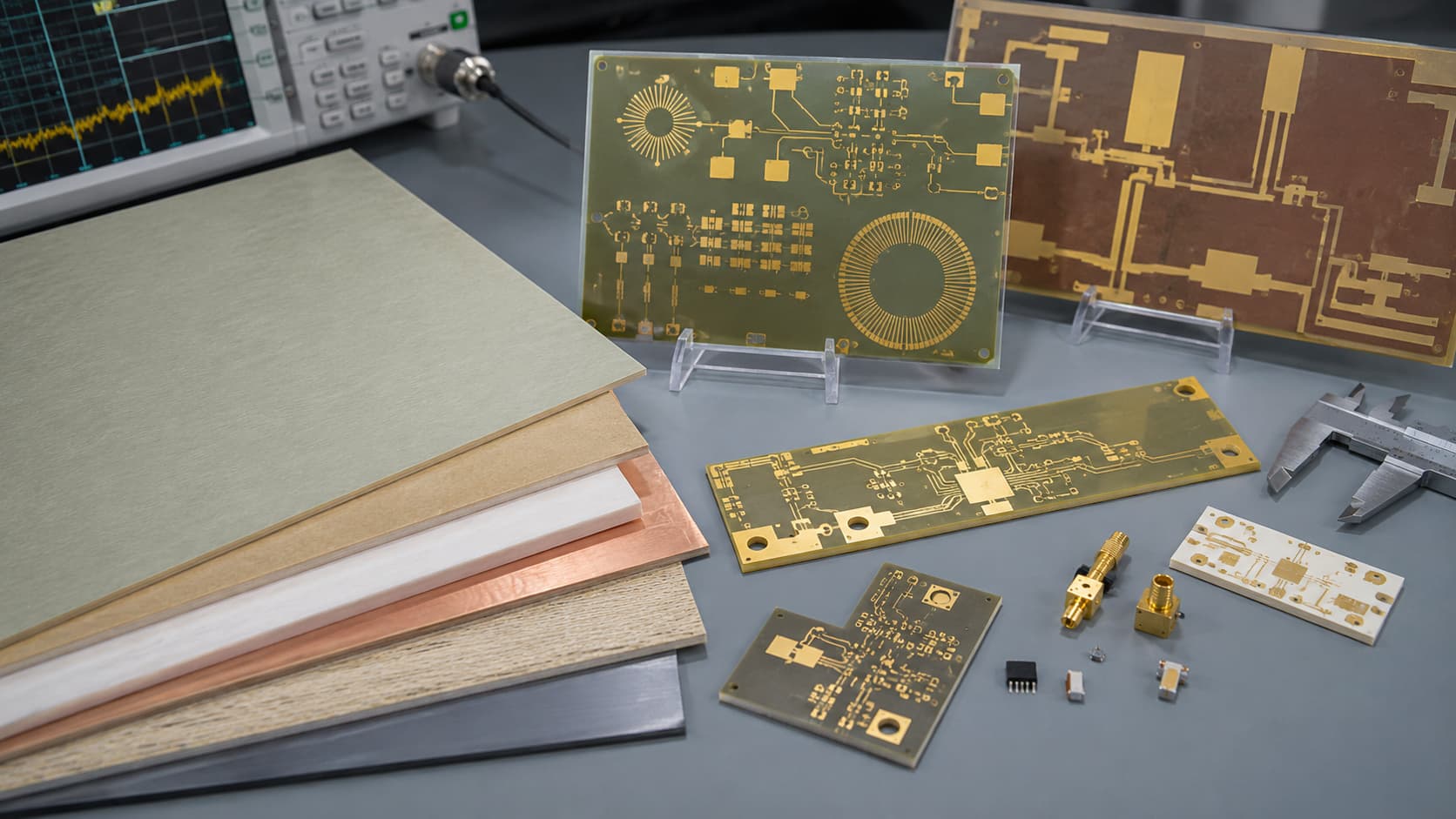
Where F4B PCB Materials Are Commonly Considered
F4B materials are usually reviewed for projects that sit between general FR4 boards and higher-end RF laminates.
Common application areas include:
RF communication boards
Antenna PCB projects
Wireless communication modules
Industrial RF equipment
Microwave signal boards
RF test fixtures
Low-volume prototype boards
Cost-sensitive high frequency circuits
For example, a basic control circuit may not need F4B. A demanding radar or satellite communication board may need Rogers, PTFE, or another lower-loss laminate. But a mid-range RF communication board or antenna circuit may fall into a zone where F4B deserves a closer look.
This is why F4B is often part of a material discussion rather than an automatic decision.
F4B vs FR4: Why the Difference Matters
FR4 is widely used because it is available, economical, and easy to process. For low-frequency control boards, power boards, and general electronic products, FR4 is often enough.
High frequency circuits are different. At higher frequencies, material loss, dielectric stability, board thickness, copper pattern accuracy, and impedance control become more visible in the final performance.
F4B may be considered when the design needs better RF behavior than standard FR4, especially in areas such as:
Antenna feed lines
RF transmission paths
Microwave signal sections
Controlled impedance traces
Wireless module circuits
Industrial RF boards
That said, F4B is not a magic solution. If the design has very strict insertion loss, phase stability, thermal reliability, or microwave performance requirements, the material should be compared carefully with other high frequency options.
F4B vs Rogers, PTFE and Taconic
In real projects, F4B is often compared with Rogers, PTFE, and Taconic materials during early material review.
Rogers materials are widely used in RF, microwave, antenna, radar, and communication applications. The official Rogers RO4000 series page is a useful benchmark when comparing high frequency material families for manufacturability and RF performance.
PTFE materials are often selected for low-loss microwave applications, radar signal paths, satellite communication, and demanding RF transmission circuits. Riching PCB’s PTFE PCB manufacturing page can help buyers understand why PTFE processing needs more manufacturing control.
Taconic materials are also used in RF and microwave PCB applications. Riching PCB’s Taconic materials page covers Taconic use cases in RF modules, microwave communication, antenna systems, radar electronics, and industrial RF equipment.
F4B may be a practical choice when the project does not need the full performance level of these premium options but still needs better high frequency behavior than FR4.
Material Parameters to Review
When reviewing F4B PCB materials, engineers should not look only at the material name.
The review should include:
Working frequency
Dk value
Df value
Board thickness
Copper thickness
Impedance target
Layer count
Surface finish
Application environment
Prototype or batch quantity
Dk affects impedance, wavelength, trace geometry, and antenna behavior. Df affects signal loss. Rogers’ technical article on dielectric constant in PCB materials is a useful reference for understanding why Dk should be reviewed carefully instead of treated as a fixed marketing number.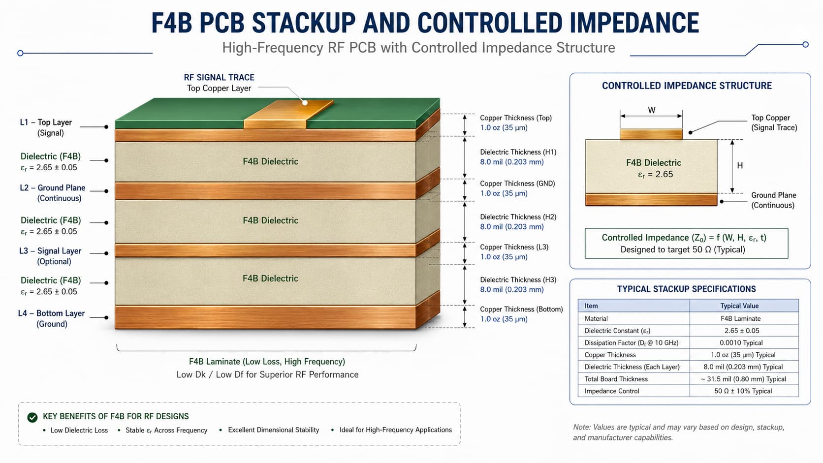
Stackup Review Before Production
F4B PCB projects should be reviewed through the stackup before manufacturing.
The stackup should clearly show:
Material type
Layer count
Dielectric thickness
Copper thickness
Signal layer
Ground plane
Power layer if used
Final board thickness
Controlled impedance target
Surface finish
Via structure
For RF PCB and microwave PCB projects, the stackup is part of the electrical design. If the dielectric thickness changes, impedance may shift. If the copper thickness changes, trace geometry may change. If the material is substituted without review, signal loss and antenna behavior may change.
This is why Riching PCB recommends reviewing RF PCB stackup design before production, especially when the project includes controlled impedance, antenna feed lines, or microwave signal paths.
Controlled Impedance with F4B PCB
Many F4B PCB projects require controlled impedance.
The most common situation is an RF transmission line or antenna feed line that needs a defined impedance, often 50 ohms. The actual value depends on the circuit and application.
Controlled impedance depends on:
Material Dk
Dielectric thickness
Trace width
Copper thickness
Ground reference
Solder mask condition
Etching tolerance
Finished board thickness
If the project has an impedance requirement, it should be stated clearly during quotation. The manufacturer should calculate impedance based on the real stackup and production tolerance.
Riching PCB’s guide on controlled impedance RF PCB manufacturing explains why impedance cannot be corrected after fabrication if the stackup and trace geometry were not planned correctly from the beginning.
Manufacturing Considerations
F4B PCB manufacturing is usually more demanding than standard FR4 fabrication, especially when the design includes RF traces, tight impedance tolerance, antenna patterns, or microwave paths.
The manufacturer should review:
Material handling
Stackup feasibility
Drilling quality
Hole wall condition
Plated through-hole reliability
Etching accuracy
Copper thickness
Surface finish
Dimensional stability
Final inspection
For simple two-layer RF boards, the key points may be material thickness, copper accuracy, and surface finish. For multilayer or hybrid boards, lamination, layer registration, and plated through-hole reliability become more important.
Surface Finish Selection
Surface finish should match the assembly method and RF requirement.
Common options include:
ENIG
Immersion silver
OSP
HASL
Lead-free HASL
Hard gold for contact areas
Customer-specified finishes
ENIG is commonly used in many RF and microwave PCB projects because it provides a flat surface and stable solderability. Immersion silver may be reviewed for some RF-sensitive applications. HASL should be selected carefully if surface flatness matters.
What Buyers Should Prepare for Quotation
A good F4B PCB quotation needs more than a quick Gerber upload.
Buyers should prepare:
Gerber files
Drill files
PCB stackup
F4B material requirement
Board thickness
Copper thickness
Surface finish
Controlled impedance requirement
Layer count
Quantity
Working frequency
Application background
Special reliability requirements
If the exact material is not confirmed, the application background becomes especially useful. A supplier can only give useful material advice when the RF requirement, frequency range, and production target are clear.
Riching PCB’s checklist on high frequency PCB quotation files can help buyers prepare a cleaner RF or microwave PCB request before sending files for review.
Common Mistakes to Avoid
The most common mistake is choosing F4B only because it is expected to reduce cost.
Other mistakes include:
No stackup review
No impedance table
Unclear working frequency
Material substitution without approval
Treating RF traces like normal copper routing
Ignoring surface finish
Missing via review
No prototype-to-batch discussion
No application background in the quotation request
F4B can be useful, but only when the design requirement and manufacturing process match the material’s real capability.
Conclusion
F4B PCB materials can be a practical option for cost-sensitive RF and microwave projects where standard FR4 is not enough, but the design may not require premium high frequency laminates across the whole board.
They may be considered for RF communication boards, antenna PCBs, wireless modules, industrial RF equipment, microwave signal circuits, and prototype projects. Still, the final choice should be based on working frequency, signal loss requirement, Dk, Df, controlled impedance, stackup design, and manufacturing feasibility.
For buyers, the best approach is simple: send complete files, explain the application, and let the manufacturer review whether F4B is suitable before production.