5G introduces a fundamental split in RF PCB requirements. Sub-6 GHz 5G (FR1) uses the same frequency range as 4G LTE but with larger antenna arrays — massive MIMO base station PCB with 64 or 128 antenna elements at 3.5 GHz requires large-panel Rogers RO4350B manufacturing capability. 5G mmWave (FR2) operates at 24–39 GHz where the antenna element dimensions are 3–6 mm, minimum line widths reach 2.5 mil, and Rogers RO3003 PTFE becomes the necessary material choice.
As a direct RF PCB factory producing both sub-6 GHz and mmWave 5G PCB, we see both application types in regular production. This guide covers the specific material, stackup, and manufacturing requirements for each.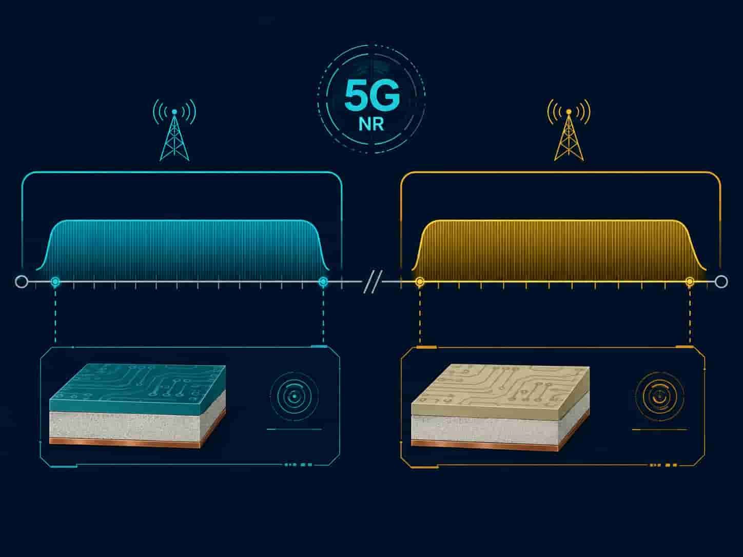
Quick Summary: Sub-6 GHz vs mmWave — Different PCB Requirements
Key point: 5G sub-6 GHz (FR1): Rogers RO4350B on large panels, standard FR4-compatible process, massive MIMO patch array with approximately 40 mm antenna element spacing at 3.5 GHz. 5G mmWave (FR2 at 28 GHz): Rogers RO3003 on 0.254 mm substrate, PTFE process required, antenna element approximately 5.4 mm, minimum line width 2.5–3 mil. 5G mmWave (FR2 at 39 GHz): Rogers RO3003 on 0.127–0.254 mm, antenna element approximately 3.8 mm, tightest manufacturing tolerance of all 5G PCB types.
5G Frequency Bands and PCB Requirements
5G NR (New Radio) is deployed across two frequency ranges with fundamentally different propagation characteristics and PCB design requirements:
FR1: Sub-6 GHz (600 MHz – 6 GHz)
FR1 provides wide area coverage and building penetration. The primary 5G NR bands for infrastructure deployment are n77 (3.3–4.2 GHz) and n78 (3.3–3.8 GHz) — the 3.5 GHz band that forms the backbone of most 5G network deployments globally.
- Primary frequency: 3.5 GHz (n77/n78 band) — most widely deployed 5G infrastructure frequency
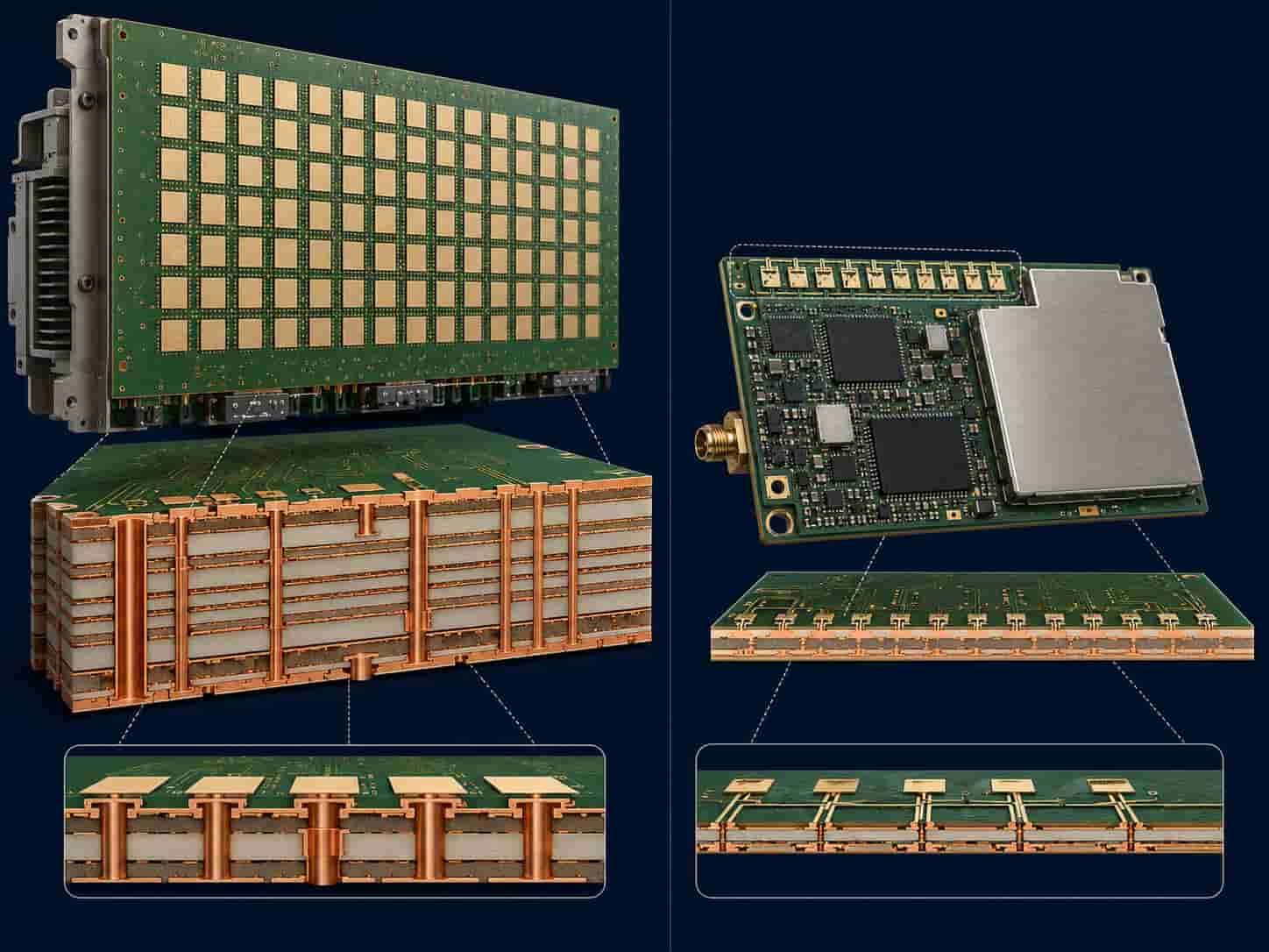
- Base station antenna PCB: massive MIMO arrays with 32T32R, 64T64R, or 128T128R configuration
- Antenna element spacing at 3.5 GHz: approximately 43 mm (λ/2)
- PCB size: large-panel, up to 480×800 mm production panel
- Material: Rogers RO4350B — adequate Df at 3.5 GHz, FR4-compatible large-panel manufacturing
- CPE (customer premises equipment): smaller PCB, same Rogers RO4350B or F4B
FR2: mmWave (24 GHz – 52 GHz)
FR2 provides very high data rates over short distances. The primary 5G NR mmWave bands are n257 (26.5–29.5 GHz), n258 (24.25–27.5 GHz), n261 (27.5–28.35 GHz), and n260 (37–40 GHz).
- n257/n258/n261 (28 GHz): antenna element ~5.4 mm on RO3003 0.254 mm substrate
- n260 (39 GHz): antenna element ~3.8 mm on RO3003 0.127–0.254 mm substrate
- PCB size: compact modules, typically 20×20 mm to 60×60 mm
- Material: Rogers RO3003 PTFE — required at mmWave for acceptable insertion loss
- Manufacturing: PTFE process required — plasma activation, minimum 2.5 mil line width
Rogers Material Selection for 5G PCB
Rogers RO4350B for Sub-6 GHz 5G
Rogers RO4350B (Dk 3.48, Df 0.0037) is the dominant material for sub-6 GHz 5G base station PCB globally. The combination of adequate RF performance at 3.5 GHz, FR4-compatible manufacturing (enabling large-panel production at established factories), and competitive cost makes RO4350B the practical choice for infrastructure-scale 5G deployment.
- Dk 3.48 at 3.5 GHz: patch antenna element ~21 mm × 21 mm
- Df 0.0037 at 3.5 GHz: insertion loss approximately 0.08 dB/cm — acceptable for base station feed networks
- Large panel production: RO4350B available in panels up to 480×800 mm — covers full massive MIMO array on single panel
- FR4-compatible process: most high-volume PCB factories can produce RO4350B — supports the scale of 5G infrastructure deployment
- Hybrid stackup: RO4350B on antenna layers + FR4 on power and digital layers — common for 5G base station PCB cost optimization
Rogers RO3003 for 5G mmWave
Rogers RO3003 (Dk 3.0, Df 0.0010) is the standard material for 5G mmWave module PCB. At 28 GHz and 39 GHz, the 73% lower Df of RO3003 compared to RO4350B translates into meaningful insertion loss advantage for the compact antenna feed networks in mmWave modules.
- Dk 3.0 at 28 GHz: 50Ω microstrip trace width ~0.56 mm (22 mil) on 0.254 mm substrate
- Dk 3.0 at 39 GHz: 50Ω microstrip trace width ~0.40 mm (16 mil) on 0.254 mm substrate — advanced manufacturing required
- Dk temperature coefficient: +13 ppm/°C — stable Dk over outdoor temperature range (-40°C to +85°C)
- PTFE process: plasma activation required — not all factories can reliably produce RO3003
- Available in 0.127 mm for highest frequency 5G mmWave designs requiring smallest antenna elements
Rogers RO3003G2 for High-Volume mmWave Production
For 5G mmWave PCB programs requiring the tightest lot-to-lot Dk consistency across large production volumes, Rogers RO3003G2 (Dk 3.0 ±0.03) provides tighter Dk tolerance than standard RO3003 (±0.04). This consistency ensures antenna resonance is reproducible across thousands of production units.
- Dk tolerance: ±0.03 vs RO3003 ±0.04 — 25% tighter
- Key benefit: more consistent antenna resonance across production lots in high-volume mmWave programs
- Processing: identical to RO3003
5G PCB Stackup Design
Sub-6 GHz Massive MIMO Base Station Stackup
A typical sub-6 GHz 5G base station PCB is a multilayer hybrid design with Rogers RO4350B on the antenna and RF signal layers and standard FR4 on the power distribution and digital control layers.
- Layer 1 (top): Rogers RO4350B — patch antenna array and RF feed network
- Layer 2: continuous copper ground plane — must not have splits under antenna or RF traces
- Layers 3–N-1: FR4 digital and power layers — routing control and power circuits
- Layer N (bottom): FR4 — digital signal routing
- Bonding film at Rogers-FR4 interface: Rogers RO4450F bondply — not standard FR4 prepreg
- Panel size: up to 480×800 mm — confirm factory capability for large-panel Rogers production
- Controlled impedance: 50Ω for RF feed lines, ±10% tolerance
5G mmWave Module Stackup
5G mmWave module PCB is a compact high-density design. The total board size is typically 20–60 mm on a side. All layers may use Rogers RO3003 or a hybrid with a single FR4 control layer on the bottom.
- Layer 1: Rogers RO3003 0.254 mm (or 0.127 mm for 39 GHz) — antenna array and RF feed
- Layer 2: continuous copper ground plane — shielding antenna from lower circuits
- Layers 3–4: Rogers RO3003 or FR4 — RF circuits, beamforming IC connections
- Minimum line width: 2.5 mil for trace widths at 28 GHz and 39 GHz on 0.254 mm substrate
- Via structure: blind vias for high-density IC connections — confirm 2-cycle PTFE limit
- Controlled impedance: ±10% for 50Ω feed lines
Manufacturing Requirements for 5G High Frequency PCB
Sub-6 GHz: Large-Panel Rogers Production
- Panel size capability: confirm factory can process RO4350B on panels up to 480×800 mm
- Lamination uniformity: large panels require even press temperature and pressure across the full panel
- Impedance coupon: placed at panel edges — confirm location and coupon design with factory
- Registration accuracy: ±0.05 mm advanced, ±0.075 mm standard — critical for large-panel patch array alignment
- Rogers RO4450F bondply: must be in factory stock — confirm before order
mmWave: Precision PTFE Manufacturing
- PTFE hole wall activation: plasma or sodium activation — ask the factory which method
- Minimum line width: 2.5 mil (0.0635 mm) — required for mmWave trace geometries on RO3003 0.254 mm
- Drill tolerance: ±0.05 mm — critical for small via pitch in mmWave modules
- Lamination: 2 press cycles maximum — strictly observed for RO3003
- Dk verification: confirm TDR impedance verification on every production panel
- Thin substrate handling: 0.127 mm RO3003 requires specialized panel handling to prevent warpage
Why Direct Factory Matters for 5G PCB
5G PCB procurement — particularly for mmWave — benefits significantly from working directly with a factory rather than through a trading company. The DFM challenges of mmWave PCB are specific and technical: confirming that 2.5 mil line widths are achievable on your specific RO3003 substrate thickness, verifying that the PTFE process is in regular production rather than occasional, and ensuring that impedance calculations use confirmed production Dk values from the material certificate rather than nominal values.
- DFM review: we recalculate impedance for every mmWave order using production Dk from material certificate
- PTFE process: plasma activation in regular production — not occasional special process
- 5 mil line width: confirmed advanced capability for mmWave module PCB
- Large panel: up to 480×800 mm for sub-6 GHz massive MIMO base station PCB
- Both sub-6 GHz and mmWave: same factory, same engineering team, same process documentation
What to Prepare for 5G High Frequency PCB Quotation
- 5G frequency band — FR1 (sub-6 GHz) or FR2 (mmWave, specify GHz)
- Application type — base station, CPE, small cell, or device module
- Rogers material grade — RO4350B for FR1, RO3003 or RO3003G2 for FR2
- Substrate thickness — standard availability depends on grade
- Panel size — especially important for large base station PCB
- Layer count and complete stackup
- Controlled impedance requirements — target and tolerance
- Minimum line width and via pitch — critical for mmWave
- IPC Class requirement
- Surface finish
- Quantity — prototype or production volume
For a complete file checklist, see What Files Are Needed for a High Frequency PCB Quotation?. For RF PCB wireless module design, see RF PCB for Wireless Communication Modules.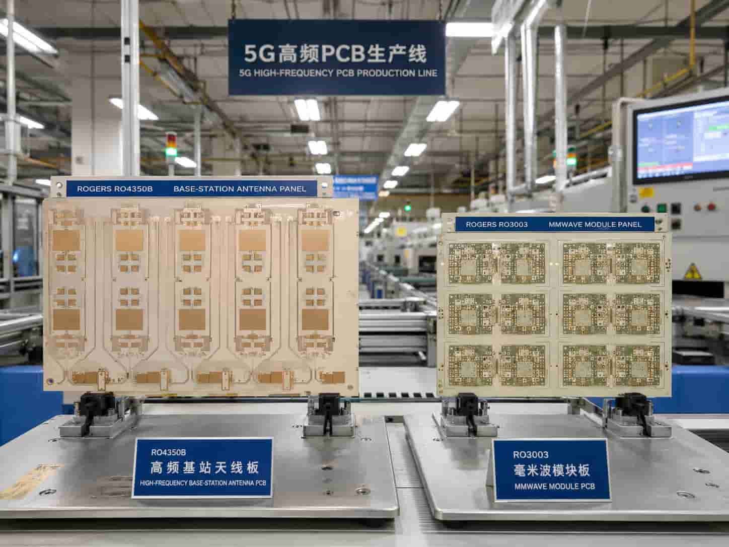
Conclusion
5G high frequency PCB spans two distinct manufacturing challenges: large-panel Rogers RO4350B production for sub-6 GHz massive MIMO base station arrays, and precision PTFE manufacturing for mmWave 28 GHz and 39 GHz front-end modules. The material, process, and dimensional requirements are fundamentally different between FR1 and FR2. Understanding which you are building — and confirming your factory has the specific capability for that type — is the starting point for reliable 5G PCB procurement.
As a direct high frequency PCB factory producing both sub-6 GHz and mmWave 5G PCB in regular production, we review every 5G PCB order with our engineering team before production — confirming material specification, impedance feasibility, and manufacturing process before your design is committed to production.