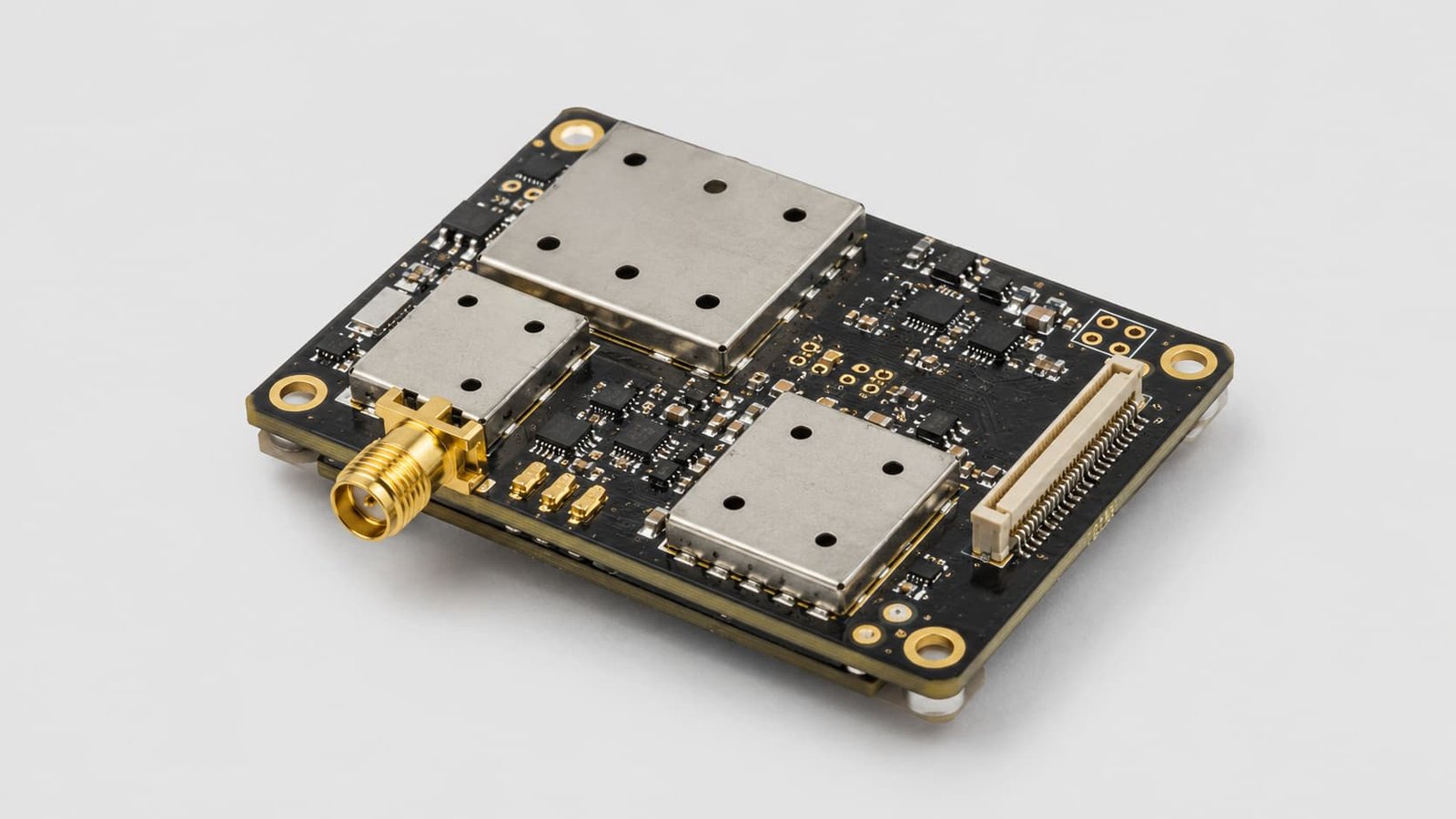
RF module PCB is used in compact wireless, communication, antenna, industrial RF, test, and signal transmission products. These boards often combine RF traces, shielding structures, connectors, grounding vias, fine-pitch components, and sometimes digital or power sections in a small layout.
For this type of PCB, the manufacturing challenge is not only making the board smaller. The real challenge is keeping RF performance stable while managing material choice, stackup, controlled impedance, connector transition, shielding, via design, and assembly quality.
For buyers, a good RF module PCB project should be reviewed before production starts. Gerber files alone may not explain the working frequency, RF path, shielding requirement, connector type, or batch consistency target.
Quick Summary
RF module PCB is used in wireless modules, communication devices, antenna systems, RF front-end circuits, industrial RF equipment, test boards, and compact signal transmission products.
These boards usually require controlled impedance, stable ground reference, reliable RF connectors, proper shielding, accurate drilling, plated through-hole quality, and careful SMT assembly.
The main risks include impedance deviation, connector mismatch, poor grounding, weak shield can soldering, via discontinuity, material substitution, and prototype-to-batch variation.
Before quotation, buyers should provide Gerber files, drill files, stackup, material requirement, working frequency, impedance details, copper thickness, surface finish, connector type, assembly needs, quantity, and application background.
Where RF Module PCBs Are Used
RF module PCBs are common in products where space is limited but RF behavior still needs to be stable.
Typical applications include:
RF front-end boards
Antenna interface modules
IoT wireless devices
Industrial RF control units
Microwave communication modules
GPS and navigation modules
RF test boards
Remote control modules
Compact signal transmission devices
Some RF modules are simple two-layer boards. Others are multilayer high frequency PCBs with RF, digital, power, and control sections on the same board. The manufacturing review should follow the RF path, not only the board size.
Material Selection
Material selection depends on working frequency, loss requirement, size, cost, and production volume.
For some lower-frequency modules, FR4 may still be acceptable if the RF trace is short and the loss requirement is not strict. For higher-frequency or more sensitive RF paths, Rogers materials, PTFE, Taconic, F4B, or hybrid stackups may need to be reviewed.
Material review should include:
Working frequency
Dk and Df values
Dielectric thickness
Copper thickness
Board thickness
Copper roughness
Material availability
Assembly temperature
Batch repeatability
In compact RF modules, the material also affects trace width. If the selected dielectric thickness makes the RF trace too wide or too narrow for practical layout, the stackup should be reviewed again.
Stackup and Controlled Impedance
RF module PCB often needs controlled impedance for transmission lines, connector paths, antenna feed lines, filters, and RF signal traces.
The stackup should define:
Layer count
Material type
Dielectric thickness
Copper thickness
RF signal layer
Ground reference plane
Power layer if used
Final board thickness
Controlled impedance target
Surface finish
Via structure
Controlled impedance should be calculated based on the real production stackup. If the material thickness or copper thickness changes during manufacturing, the impedance may shift.
In compact modules, this risk is easy to miss because the board is small. But short RF paths can still fail if the connector launch, trace geometry, or reference plane is poorly controlled.
Grounding and Shielding
Grounding is one of the most important parts of RF module PCB design.
A stable ground reference helps control return current, reduce radiation, improve shielding, and support predictable impedance. Shielding cans are often used to isolate RF sections from digital noise, nearby components, or external interference.
The review should include:
Ground plane continuity
Ground stitching vias
Via fence spacing
Shield can pad design
Solder mask opening
Copper clearance
Ground connection to enclosure
RF section isolation
Shielding is not only an assembly item. The PCB must provide proper pads, ground vias, and solderable areas for the shield can. If the shield structure is weak, RF isolation and mechanical reliability may suffer.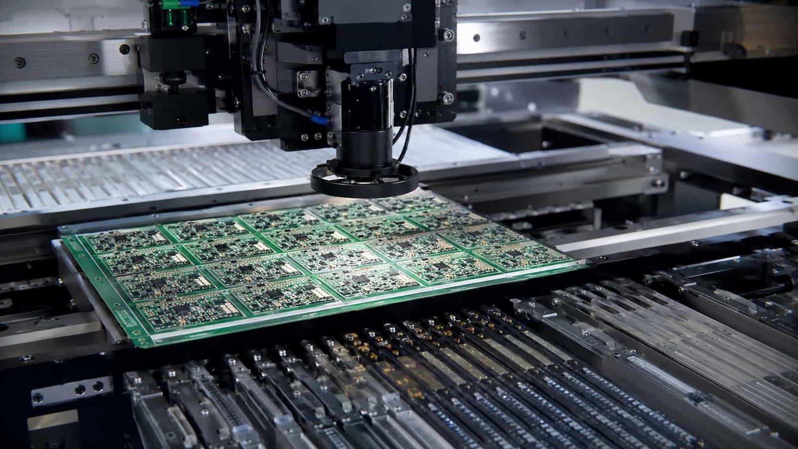
RF Connectors and Board Interfaces
RF module PCBs may use SMA, U.FL, IPEX, board-to-board RF connectors, edge contacts, coaxial cable interfaces, or custom connector structures.
Connector areas should be reviewed carefully because they affect both electrical performance and mechanical reliability.
Important review points include:
Connector footprint
Pad-to-trace transition
Ground via placement
Reference plane continuity
Cable stress
Mounting strength
Connector height
Assembly process
Surface finish
A good RF trace can still perform poorly if the connector launch is wrong. In compact modules, the connector area may be close to shields, mounting holes, or other components, so layout and manufacturing tolerance become more sensitive.
Via Design and Layer Transitions
Vias may be used for RF signal transition, grounding, shielding, thermal transfer, and component connection.
For RF module PCB, via design should not be treated as a simple routing detail. Poor via placement can affect impedance, isolation, and return path.
The review should include:
Signal via size
Ground via spacing
Via fence design
Via stub length
Anti-pad clearance
Plated through-hole reliability
Shielding via connection
Layer transition path
If the module uses a multilayer structure, the signal transition between layers should be reviewed before production. A via-related problem is difficult to fix after the board is fabricated.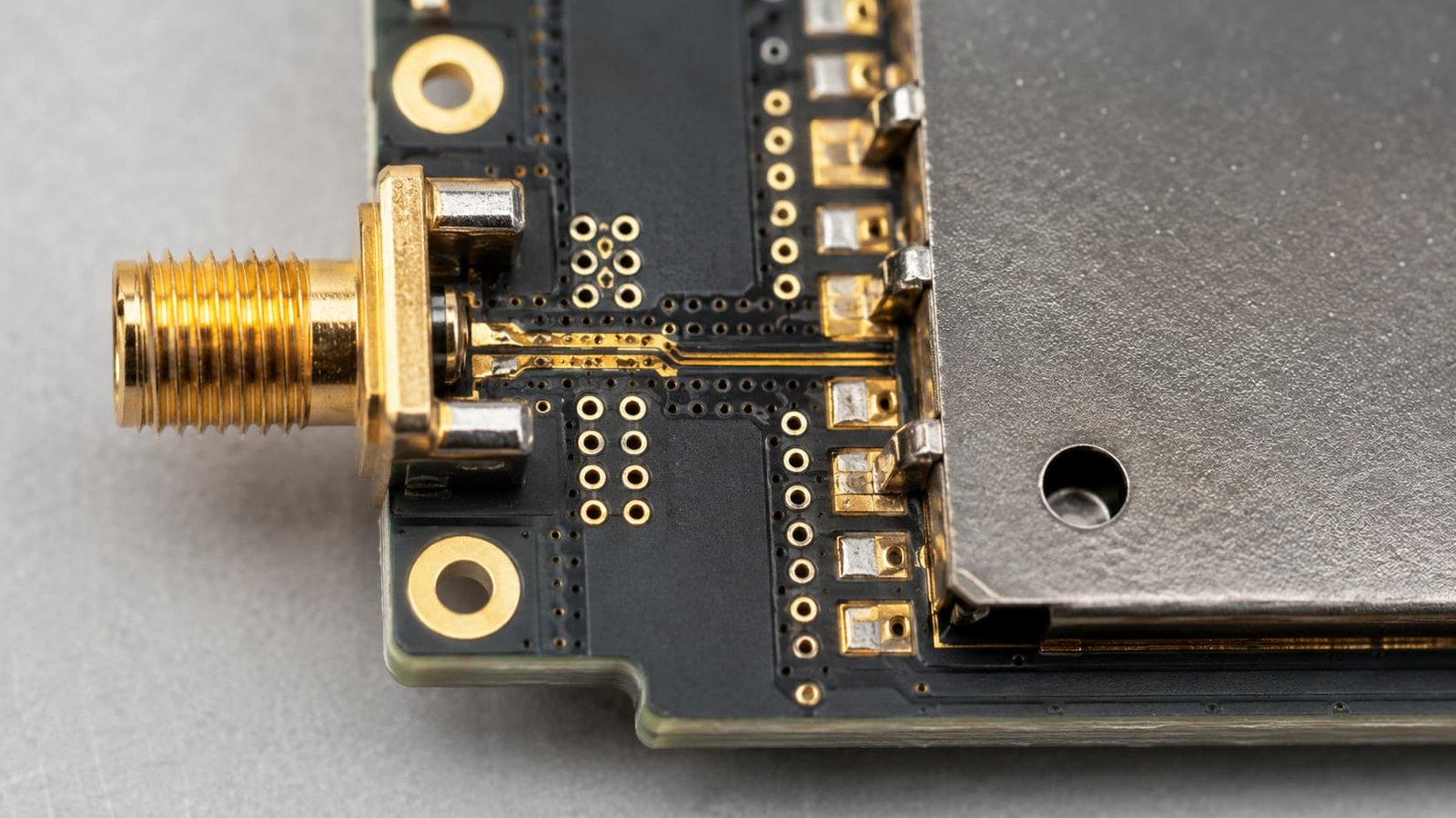
SMT Assembly and Component Placement
Many RF modules use small components, fine-pitch pads, shields, connectors, and compact component spacing. This makes assembly review important.
The manufacturer should check:
Component spacing
Solder paste opening
Shield can solder area
Connector assembly method
Thermal profile
Small passive placement
Board warpage risk
Panelization for assembly
Inspection access
RF performance can be affected by assembly quality. Poor soldering around connectors, shields, filters, or matching components may create unstable results even if the bare PCB is correct.
If the project includes both PCB fabrication and assembly, the assembly requirement should be discussed early.
Surface Finish
Surface finish affects solderability, RF pads, connector areas, storage, and assembly reliability.
Common options include:
ENIG
Immersion silver
OSP
Lead-free HASL
Hard gold for contact areas
Customer-specified finishes
ENIG is often selected for RF modules because it provides a flat surface and stable solderability. Hard gold may be needed for contact areas or repeated mating. Immersion silver may be reviewed for some RF-sensitive designs.
The finish should match the RF requirement, component assembly, connector structure, and storage condition.
Prototype-to-Batch Consistency
RF modules often move from prototype to batch production. A successful sample does not guarantee stable repeat orders.
Batch risk may come from:
Material substitution
Stackup change
Copper thickness variation
Different surface finish
Connector source change
Shield can assembly variation
Panelization change
No impedance test requirement
Buyers should confirm whether the approved material, stackup, impedance, and assembly process can be repeated in future orders. For RF modules, small production changes may create measurable performance differences.
What Buyers Should Provide for Quotation
A complete quotation package helps reduce engineering delay and RF risk.
Buyers should prepare:
Gerber files
Drill files
PCB stackup
Material requirement
Working frequency
Controlled impedance table
Board thickness
Copper thickness
Surface finish
Connector type
Shielding requirement
Assembly requirement if needed
Quantity
Prototype or batch plan
Application background
If the material is not fixed, the working frequency and application background are especially useful. The manufacturer can then review whether FR4, Rogers, PTFE, Taconic, F4B, or a hybrid stackup is more practical.
Common Mistakes to Avoid
Common mistakes include:
Treating the RF module as a normal small PCB
Sending files without stackup
No controlled impedance table
Ignoring connector launch areas
Using too few ground vias
Weak shield can pad design
Changing material after prototype
Choosing surface finish by habit
Not discussing assembly process
Ignoring batch repeatability
These problems may not appear during visual inspection. They often appear during RF testing, assembly, or repeat production.
Conclusion
RF module PCB manufacturing requires careful review of material, stackup, controlled impedance, connector launch, grounding, shielding, vias, surface finish, assembly process, and batch consistency.
For compact wireless modules, RF front-end boards, antenna interfaces, industrial RF devices, and communication products, the PCB is part of the RF system. It should not be treated as a standard small circuit board.
The best results come when buyers provide complete files, working frequency, impedance requirements, connector details, shielding information, assembly needs, and application background before production begins.