RF PCB for wireless communication modules requires controlled 50Ω impedance, a low-loss laminate matched to the operating frequency, and TDR-verified manufacturing. The substrate choice determines how much signal you lose between transmitter and antenna — a decision that cannot be corrected after layout.
For WiFi 6 and WiFi 6E modules operating at 2.4 GHz, 5 GHz, and 6 GHz: Rogers RO4350B (Dk 3.48, Df 0.0037) is the standard material. For 5G sub-6GHz RF front-end modules: RO4350B or RO4003C (Df 0.0027). For mmWave 5G at 28 GHz and above: Rogers RO3003 (Dk 3.0, Df 0.0010) or RT5880 (Dk 2.2, Df 0.0009). For Bluetooth, Zigbee, LoRa and lower-power IoT modules below 1 GHz: FR4 + Rogers hybrid stackup is often sufficient and reduces cost.
Riching PCB manufactures RF PCB for wireless communication modules from prototype (1 board, no MOQ) through production. Rogers RO4350B, RO4003C, RO3003, RT5880, Taconic and F4B materials in stock. Controlled impedance ±10% standard, TDR verification available. Prototype lead time 5–7 working days.
Quick Summary
RF PCB for wireless communication modules is commonly used in RF modules, antenna circuits, wireless devices, IoT products, RF front-end boards, communication equipment, and test systems.
The most important RF PCB requirements include controlled impedance, low signal loss, stable dielectric performance, accurate copper geometry, proper grounding, and reliable plated through holes.
Common material options include Rogers, PTFE, Taconic, F4B, and FR4 plus high frequency hybrid stackups.
For wireless communication PCB projects, Riching PCB supports RF PCB manufacturing, high frequency PCB production, microwave PCB manufacturing, antenna PCB manufacturing, and RF Communication PCB manufacturing for RF modules, antenna systems, signal transmission boards, and wireless devices. Riching PCB’s RF communication page describes support for high frequency PCB, RF PCB, microwave PCB, antenna PCB, and hybrid PCB manufacturing for RF communication modules and wireless devices.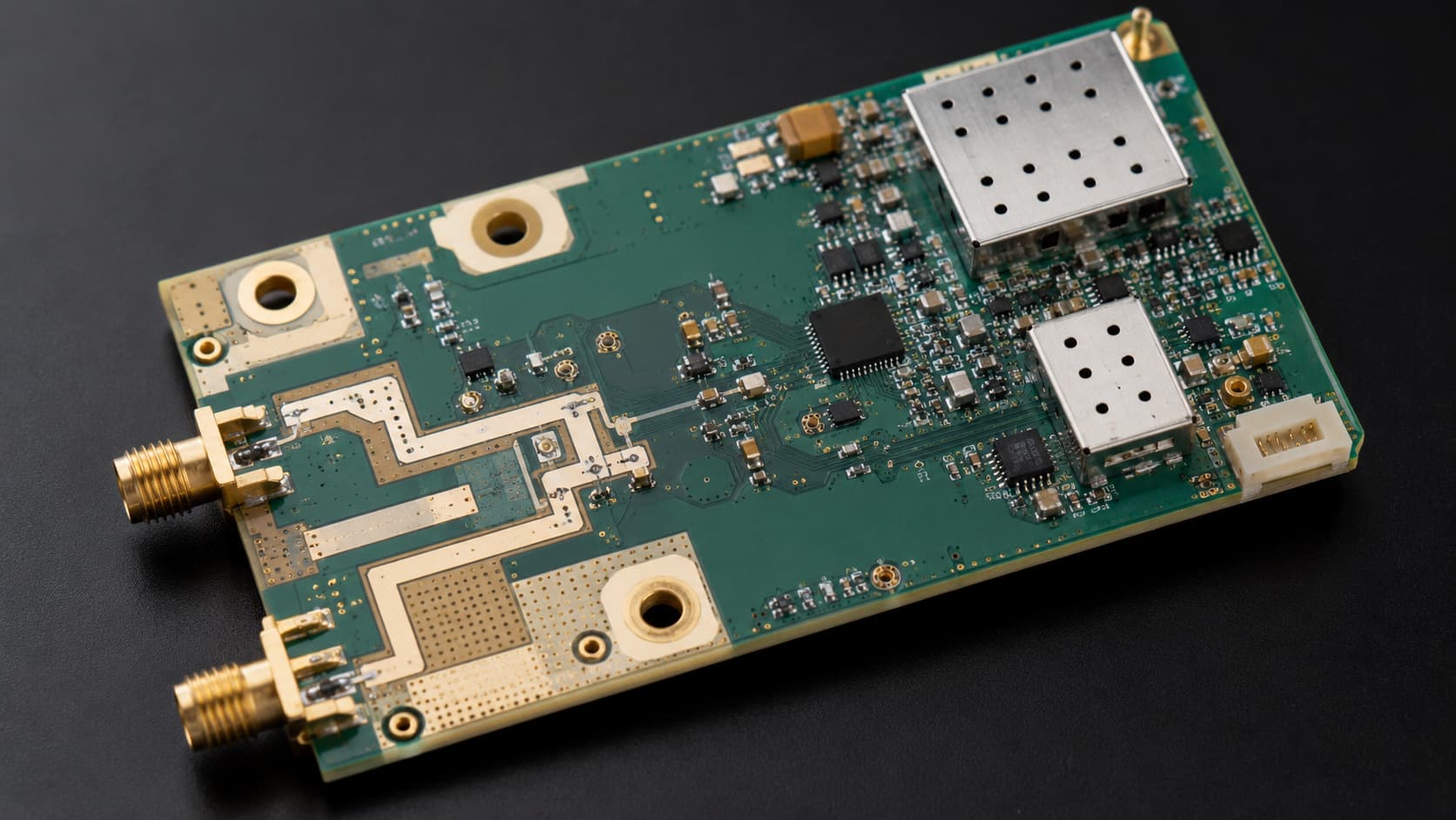
Why Wireless Communication Modules Need RF PCB
Wireless communication modules transmit and receive RF signals. These signals are sensitive to impedance mismatch, signal loss, material variation, trace geometry, grounding structure, and antenna feed design.
If the PCB is not designed or manufactured properly, the module may suffer from weak signal performance, unstable communication distance, poor antenna matching, unwanted noise, or inconsistent RF testing results.
RF PCB is commonly used in wireless communication applications such as:
WiFi modules
Bluetooth modules
IoT wireless modules
RF front-end boards
Antenna matching circuits
Industrial wireless devices
Remote control systems
RF amplifiers
Communication equipment
Test and measurement devices
Key Requirements for RF PCB in Wireless Modules
Controlled Impedance
Controlled impedance is one of the most important requirements in RF PCB manufacturing.
Many wireless communication modules use RF transmission lines that need a target impedance, commonly 50 ohms. If the actual impedance is not controlled, signal reflection and power loss may occur.
Controlled impedance depends on:
Material Dk
Dielectric thickness
Trace width
Copper thickness
Reference ground plane
Solder mask
Stackup structure
Manufacturing tolerance
Texas Instruments’ SimpleLink Wi-Fi hardware design guide refers to a 50-ohm controlled impedance trace for RF routing, which is a useful technical reference when explaining wireless module PCB layout requirements.
Low Signal Loss
Wireless communication modules need stable signal transmission between RF components, antennas, connectors, filters, amplifiers, and matching circuits.
If the PCB material has high loss, part of the RF signal may be absorbed or weakened during transmission. This can reduce module performance, communication stability, and signal range.
Low-loss PCB materials are often considered for RF modules, especially when the working frequency is higher or the product requires reliable wireless performance.
Rogers describes its RO4000 series laminates as low-loss materials used in microwave and millimeter-wave frequencies, with easier circuit fabrication compared with traditional PTFE-based microwave materials. This makes Rogers RO4000 a useful external reference for RF and wireless communication PCB material selection.
Stable Stackup Design
The RF PCB stackup affects impedance, signal loss, grounding, crosstalk, and module reliability.
For wireless communication modules, the stackup should confirm:
Layer count
Material type
Dielectric thickness
Copper thickness
RF signal layers
Ground plane location
Power plane structure
Antenna feed line structure
Controlled impedance target
Final board thickness
Surface finish
A stable ground reference is especially important for RF signal paths. If the ground plane is broken or poorly connected, RF performance may become unstable.
Before production, the PCB manufacturer should review whether the proposed stackup can meet the impedance requirement and manufacturing tolerance.
Material Selection for Wireless Communication RF PCB
Material selection directly affects RF PCB performance.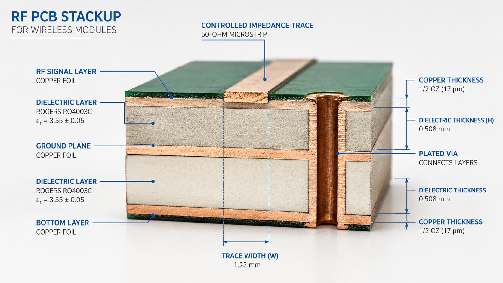
Different wireless communication modules may need different materials depending on frequency, signal loss requirement, module size, antenna structure, layer count, and cost target.
Common RF PCB material options include Rogers, PTFE, Taconic, F4B, and FR4 plus high frequency hybrid stackups.
Rogers Materials
Rogers materials are widely used in RF, microwave, antenna, radar, satellite communication, and wireless infrastructure applications.
For wireless communication modules, Rogers materials may be selected when the design requires stable electrical performance, controlled impedance, lower signal loss, and better high frequency behavior than standard FR4.
Riching PCB’s Rogers Materials page is a strong internal link target here because it explains Rogers material support for RF, microwave, antenna, radar, satellite communication, wireless infrastructure, and other high frequency PCB applications.
PTFE Materials
PTFE materials are often used in low-loss RF and microwave applications.
For wireless communication modules with higher frequency, stricter signal loss requirements, or demanding antenna performance, PTFE laminates may be considered.
However, PTFE PCB manufacturing is more difficult than standard FR4. Drilling, plating, bonding, lamination, and dimensional stability require experienced process control.
Taconic Materials
Taconic materials can also be used in RF and microwave PCB projects.
For wireless communication modules, Taconic materials may be suitable when the project requires stable dielectric performance, low signal loss, and high frequency material support.
Riching PCB’s Taconic Materials page describes Taconic materials as suitable for RF modules, microwave communication boards, antenna systems, radar electronics, wireless infrastructure, and industrial high frequency PCB applications.
F4B Materials
F4B materials may be considered for cost-sensitive RF PCB projects.
For some wireless communication modules, F4B can provide better high frequency performance than standard FR4 while helping balance cost, material availability, and production efficiency.
However, F4B should still be reviewed based on operating frequency, signal loss requirement, impedance control, and stackup feasibility.
FR4 + High Frequency Hybrid Stackups
Not every wireless communication module requires high frequency material across the entire board.
Some multilayer RF PCB designs use high frequency materials only on critical RF layers, while using FR4 for supporting layers. This type of hybrid stackup can help balance performance, mechanical strength, and cost.
However, hybrid stackups require careful review because different materials may have different thermal expansion, bonding behavior, and lamination requirements.
RF Transmission Lines in Wireless Modules
RF transmission lines are critical in wireless communication module PCB design.
Common RF transmission line structures include:
Microstrip
Stripline
Coplanar waveguide
Grounded coplanar waveguide
Antenna feed line
Controlled impedance RF trace
The final structure depends on layer count, board thickness, antenna design, material Dk, and impedance target.
TI’s PCB trace impedance reference explains that characteristic impedance is determined by trace geometry, which supports the importance of trace width, dielectric thickness, and stackup control in RF PCB design.
For RF module PCBs, the manufacturer should avoid uncontrolled trace width changes, broken reference planes, poor ground via placement, and unnecessary routing discontinuities.
Antenna Feed Line Design
Antenna feed lines connect RF circuits to antennas or RF connectors. In many wireless communication modules, antenna feed line performance directly affects signal transmission and antenna matching.
The antenna feed line should be designed with controlled impedance and a stable ground reference. If the feed line impedance is not correct, the module may show poor signal performance or unstable antenna efficiency.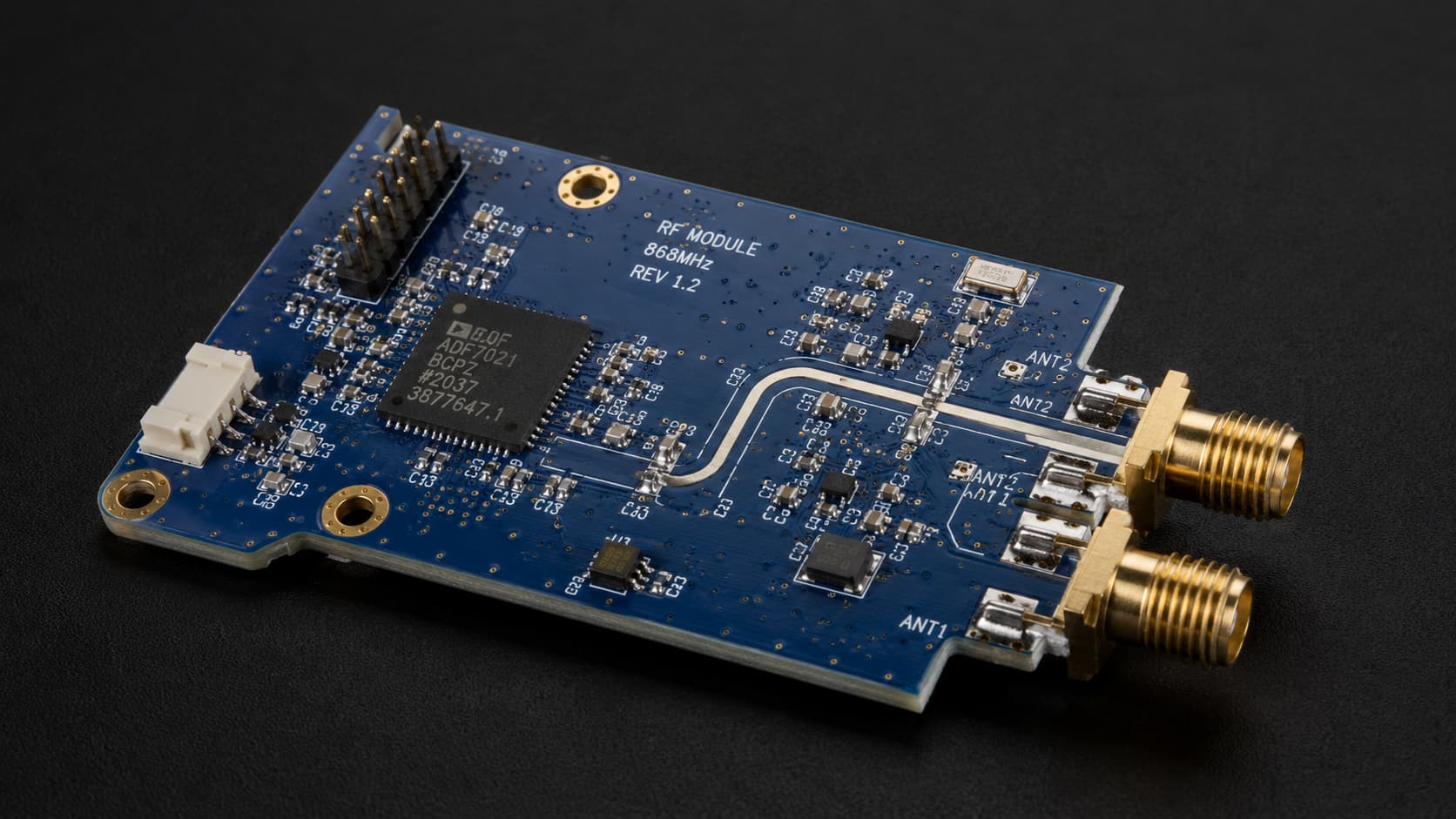
Grounding and Via Design
Grounding is very important in RF PCB manufacturing.
A strong ground reference helps reduce unwanted noise, stabilize impedance, and improve RF signal return paths. Ground vias are often placed near RF traces, connectors, shielding areas, and antenna feed structures.
For wireless communication modules, via design should consider:
Ground via placement
Via spacing
RF return path
Shielding structure
Signal isolation
Thermal performance
Plated through-hole reliability
Poor grounding may cause unstable wireless performance, unwanted coupling, noise, or RF testing problems.
RF Front-End PCB in Wireless Communication Modules
Wireless communication modules may include RF front-end circuits such as filters, low-noise amplifiers, power amplifiers, switches, matching networks, and antenna feed structures.
These circuits require careful PCB layout and reliable manufacturing control.
For RF front-end PCB projects, the manufacturer should review:
Material selection
RF path length
Impedance control
Grounding structure
Copper thickness
Via design
Thermal behavior
Surface finish
Connector footprint
Assembly requirements
If the board includes power amplifier areas, copper thickness, heat dissipation, and plated through-hole reliability may become more important.
Wireless Module PCB Manufacturing Challenges
RF PCB manufacturing for wireless modules is more complex than standard PCB fabrication.
Important manufacturing challenges include:
Material thickness control
Copper thickness control
Trace width accuracy
Etching tolerance
Controlled impedance production
Accurate drilling
Stable plated through holes
Multilayer lamination
Surface finish consistency
Dimensional stability
Engineering review before production
For RF PCB projects, small variations in dielectric thickness, trace width, or copper thickness can affect impedance and RF performance. Therefore, stackup and material changes should be reviewed before production.
Surface Finish for RF PCB
Surface finish affects solderability, assembly quality, and sometimes RF performance.
Common surface finish options may include immersion gold, immersion silver, OSP, HASL, or other customer-specified finishes.
For many RF and microwave PCB projects, immersion gold is often considered because it provides a flat surface and stable soldering performance. However, the final surface finish should be selected based on the module design, assembly process, RF requirement, and customer specification.
What Files Are Needed for RF Module PCB Quotation?
To quote an RF PCB for wireless communication modules accurately, the manufacturer usually needs complete engineering information.
Recommended files and details include:
Gerber files
Drill files
PCB stackup
Material requirement
Working frequency
Board thickness
Copper thickness
Surface finish
Controlled impedance requirement
Layer count
Quantity
Prototype or batch production requirement
Application background
Special tolerance or reliability requirements
If the material is not confirmed, the manufacturer can help review whether Rogers, PTFE, Taconic, F4B, FR4, or a hybrid stackup is more suitable.
How to Reduce Risk Before RF PCB Production
To reduce risk before RF PCB manufacturing, engineers and buyers should confirm:
Working frequency is clear
Material requirement is confirmed
Stackup is reviewed
Controlled impedance values are defined
Antenna feed line structure is checked
Ground reference is continuous
Copper thickness is confirmed
Drill and via structures are reviewed
Surface finish is selected
Prototype and batch requirements are clear
Engineering review is completed before production
For wireless communication modules, material substitution should not be made casually. A material with similar Dk may still behave differently because of Df, thickness tolerance, copper type, processing behavior, and availability.