
High frequency PCB material selection is not only about choosing a famous laminate name. For RF PCB, microwave PCB, antenna PCB, radar electronics, and communication boards, the material affects impedance, signal loss, antenna behavior, stackup design, drilling, plating, surface finish, and production repeatability.
Many problems happen because the material is selected too early, too cheaply, or without enough manufacturing review. A board may pass basic fabrication checks but fail RF testing because the material, stackup, copper thickness, or impedance assumptions were not aligned.
For buyers, the safest material decision is not always the most expensive option. It is the material that matches the working frequency, signal path, manufacturing process, availability, and batch production plan.
Quick Summary
High frequency PCB material selection should be based on working frequency, Dk, Df, dielectric thickness, copper thickness, stackup, impedance target, loss requirement, application environment, and production quantity.
Common mistakes include choosing material only by price, treating all Rogers or PTFE materials as interchangeable, ignoring Dk tolerance, changing material after layout, and sending files without stackup details.
A material that works in prototype may still create batch risk if availability, laminate thickness, copper type, or manufacturing process changes later.
Before quotation, buyers should provide Gerber files, drill files, stackup, material preference, working frequency, impedance requirement, copper thickness, surface finish, quantity, and application background.
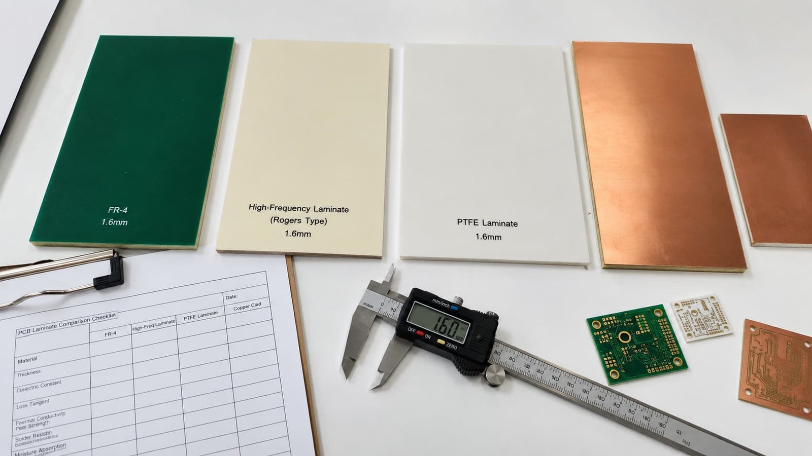
Mistake 1: Choosing Material Only by Price
Cost matters, but price alone is a poor way to choose high frequency PCB material.
A cheaper material may look attractive during quotation, but it can increase the total project cost if it causes signal loss, impedance shift, tuning problems, failed testing, or repeated prototypes.
Material price should be reviewed together with:
Working frequency
Signal loss requirement
Dk and Df values
Stackup feasibility
Controlled impedance
Material availability
Processing difficulty
Batch repeatability
For simple RF boards, a cost-balanced material may be enough. For microwave signal paths, antenna feed networks, or radar-related circuits, a lower-cost material may create more risk than savings.
Mistake 2: Treating Material Names Too Broadly
Some buyers write only “Rogers material,” “PTFE material,” or “high frequency laminate” in the quotation request. This is too broad.
Different material families can have different Dk, Df, copper types, thickness options, drilling behavior, and processing requirements. Even materials from the same supplier may not be interchangeable.
A useful material request should include the exact material type when possible. If the exact material is not fixed, the buyer should provide the working frequency, impedance target, loss requirement, and application background so the manufacturer can review practical options.
Mistake 3: Ignoring Dk and Df Tolerance
Dk and Df are often listed in datasheets, but buyers should not treat them as simple fixed numbers.
Dk affects trace width, impedance, wavelength, antenna size, and phase behavior. Df affects dielectric loss. For high frequency RF and microwave boards, these values are tied to real signal performance.
The review should include:
Nominal Dk
Dk tolerance
Df value
Frequency condition
Dielectric thickness
Copper type
Stackup structure
If the design is sensitive, the material should be reviewed based on the actual frequency and stackup, not only a general datasheet value.
Mistake 4: Separating Material Selection From Stackup
Material and stackup should be reviewed together.
A good material can still create problems if the dielectric thickness is wrong, the copper thickness changes, or the ground reference does not match the impedance calculation.
The stackup should define:
Layer count
Material type
Dielectric thickness
Copper thickness
RF signal layer
Ground reference plane
Final board thickness
Controlled impedance target
Surface finish
Via structure
For RF and microwave PCB projects, stackup is part of the electrical design. It should not be finalized after the material is purchased.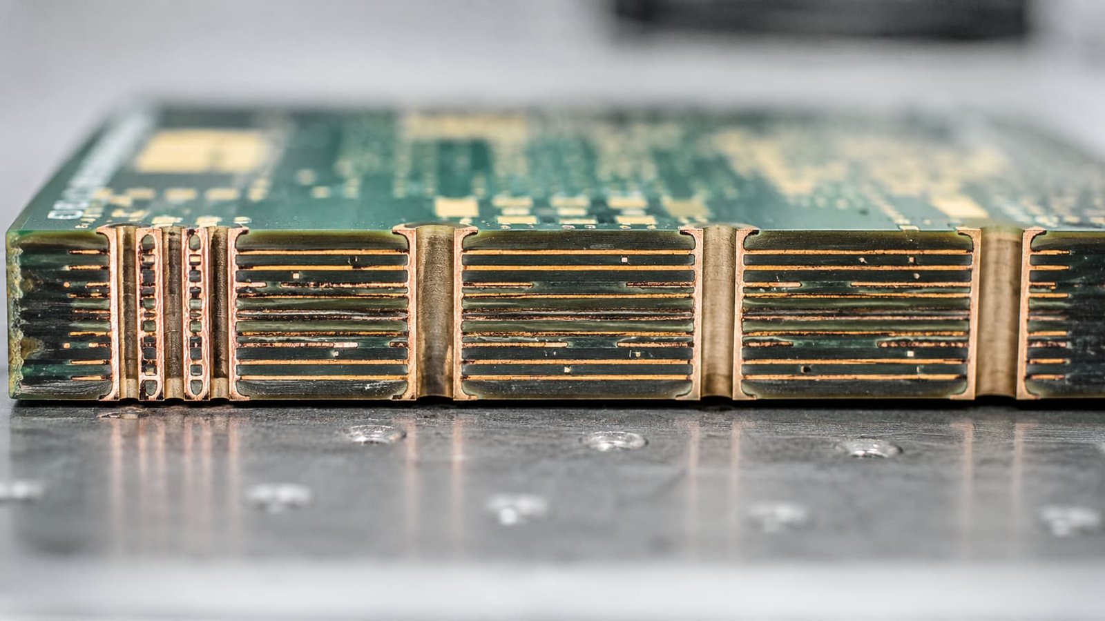
Mistake 5: Changing Material After Layout
Material substitution after layout is risky.
If the layout was designed around one material Dk and thickness, changing to another material may affect trace width, impedance, antenna tuning, and signal loss. This is especially risky for antenna PCB, microwave PCB, and controlled impedance RF boards.
A material change should trigger engineering review of:
Dk difference
Df difference
Dielectric thickness
Trace width
Impedance calculation
Antenna or RF tuning
Via transitions
Surface finish
Testing plan
Material substitution may be possible, but it should never be treated as a simple purchasing adjustment.
Mistake 6: Ignoring Manufacturing Difficulty
Some high frequency materials are more difficult to process than standard FR4.
Manufacturing difficulty may appear in:
Drilling quality
Hole wall preparation
Plating reliability
Copper adhesion
Dimensional stability
Lamination behavior
Etching tolerance
Panel handling
Surface finish control
PTFE-based materials, hybrid stackups, and some low-loss laminates may require more process control. If the factory is not familiar with the material, the board may look acceptable but create long-term reliability or RF performance problems.
Mistake 7: Forgetting Prototype-to-Batch Consistency
Many buyers focus on the first prototype and forget repeat production.
A prototype can pass testing, but the batch version may change because of material availability, different thickness options, copper variation, changed panelization, or supplier substitution.
Before approval, buyers should confirm:
Can the material be supplied for future orders?
Is the same thickness available for batch production?
Will the stackup remain unchanged?
Is impedance testing required for batch orders?
Can the same surface finish be used again?
Does the factory understand the RF requirement?
For B2B projects, repeatability is often more valuable than a one-time successful sample.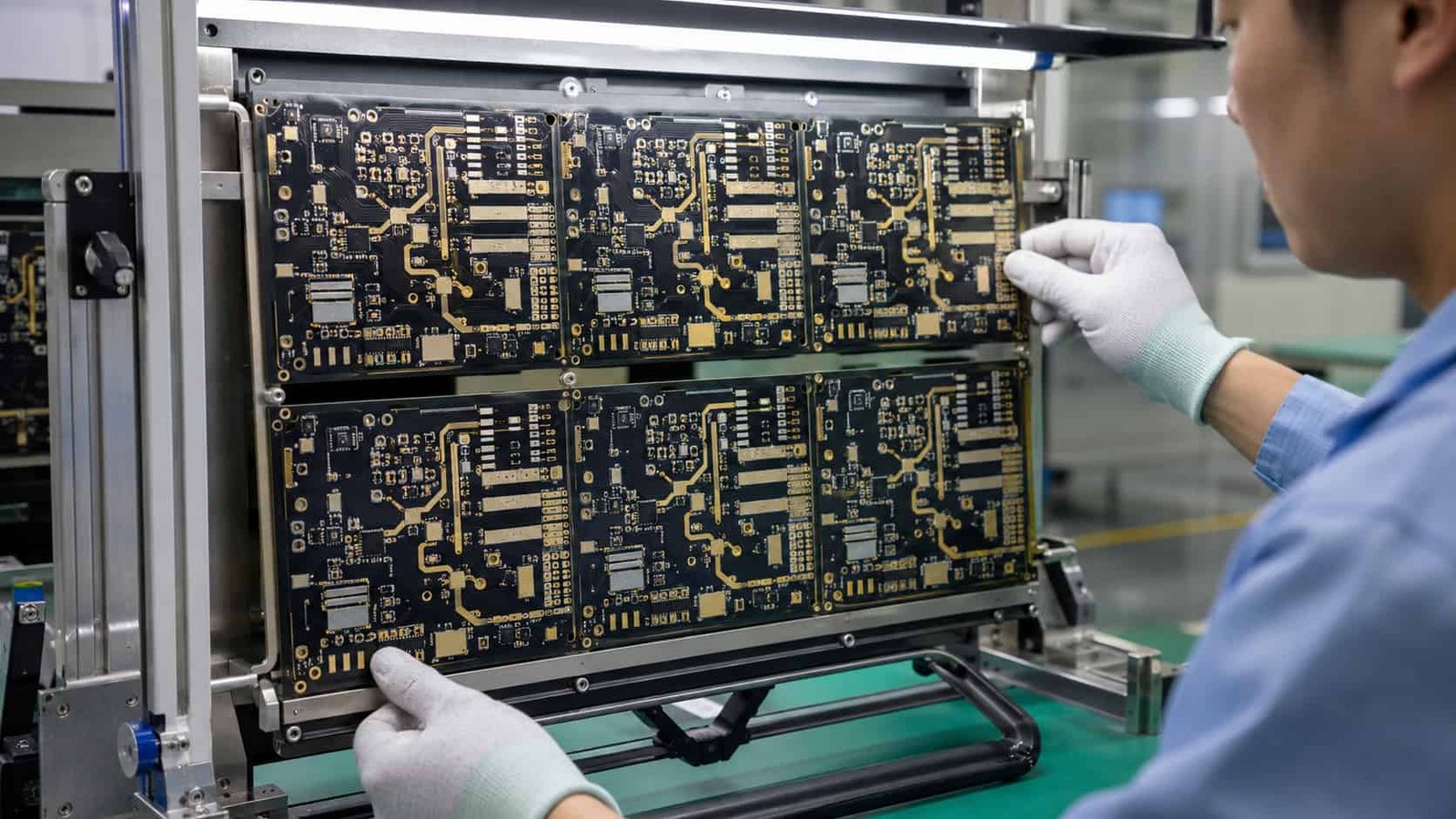
Mistake 8: Not Providing Application Background
Gerber files show the board geometry, but they do not explain the RF requirement.
Without application background, the manufacturer may not know whether the board is used for antenna feed, RF power, microwave communication, radar electronics, satellite communication, or test equipment. These applications can have different material risks.
Buyers should provide:
Working frequency
Signal type
Application area
Impedance requirement
Loss sensitivity
Prototype or batch plan
Special assembly requirement
Operating environment
This information helps the manufacturer review whether the requested material is reasonable or whether another option should be discussed.
What Buyers Should Prepare Before Quotation
A complete quotation request should include:
Gerber files
Drill files
PCB stackup
Material preference
Working frequency
Controlled impedance requirement
Board thickness
Copper thickness
Surface finish
Quantity
Prototype or batch plan
Application background
Special reliability requirement
If the buyer is not sure which material to choose, the working frequency and application background are the most useful starting points.
Conclusion
High frequency PCB material selection should not be handled like standard PCB material selection. For RF PCB, microwave PCB, antenna PCB, radar electronics, and communication boards, the material affects signal behavior, impedance, loss, manufacturing difficulty, and batch repeatability.
The most common mistakes are choosing material only by price, using broad material names, ignoring Dk and Df tolerance, separating material from stackup, changing material after layout, and forgetting prototype-to-batch risk.
A better approach is to review material, stackup, impedance, manufacturing process, availability, and application requirement before production starts. This reduces RF testing risk and helps the finished PCB perform as expected, not just look correct.