Radar systems are among the most demanding applications for high frequency PCB. From ground-based early warning radar operating at L-band and S-band to airborne fire control radar at X-band, electronic warfare systems spanning the full microwave spectrum, and active electronically scanned array (AESA) radar at Ka-band and W-band, every radar type places different and specific requirements on the PCB material, stackup design, and manufacturing process.
The high frequency PCB inside a radar system carries the transmit and receive signal path, the antenna feed network, the transmit/receive (T/R) module electronics, the local oscillator distribution, and the signal processing front-end. Each of these functions has different frequency, power handling, isolation, and reliability requirements — often on the same board or in the same module assembly.
This guide covers the high frequency PCB requirements for key radar system types, material selection by frequency band, AESA phased array design considerations, electronic warfare PCB requirements, and what to confirm before production for defense radar projects.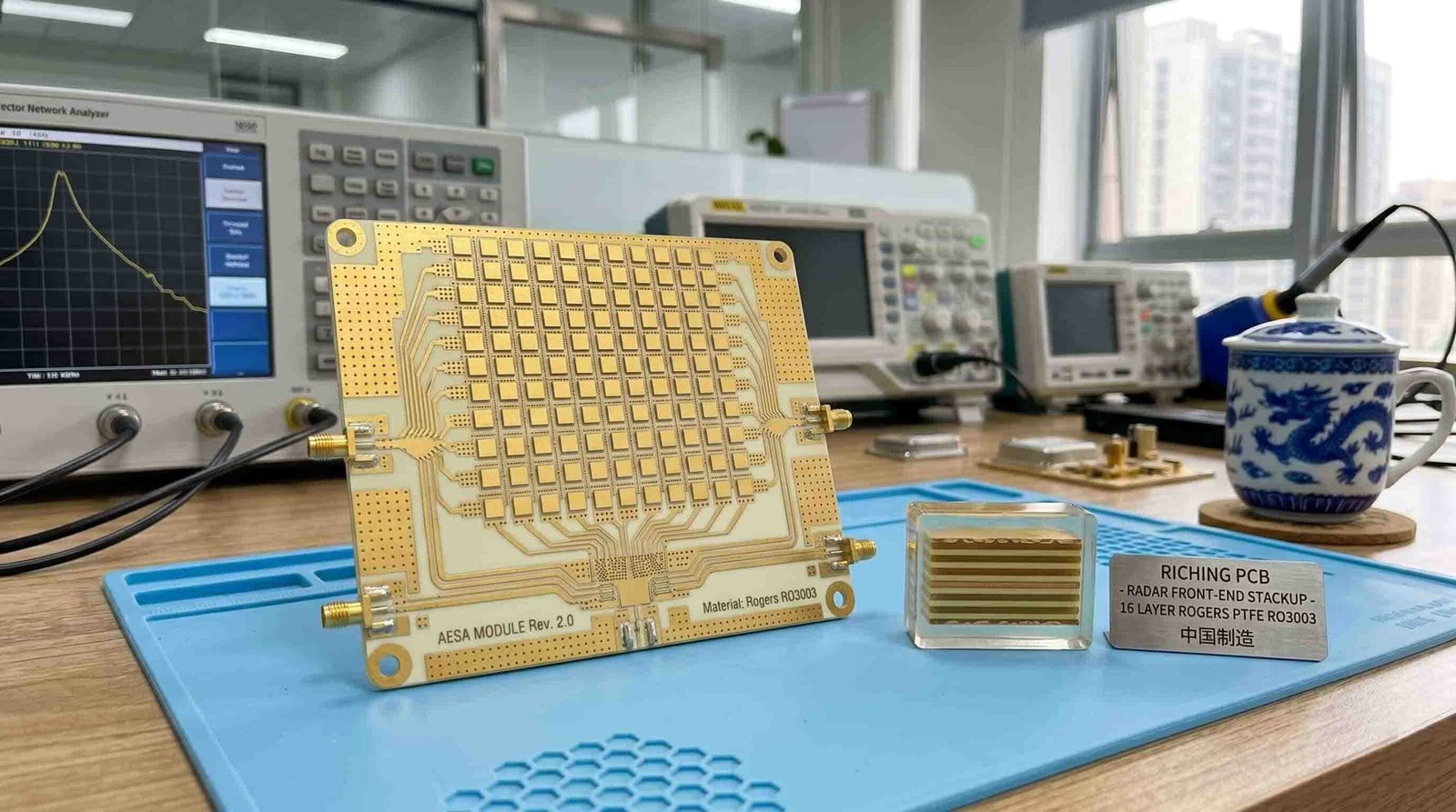
Quick Summary
Key point: Radar system PCB material selection depends primarily on the operating frequency band and insertion loss requirement. Rogers RO4350B covers most L-band to X-band applications. Rogers RO3003 and RT5880 are required for Ka-band, W-band, and low-loss EW applications. AESA phased array PCB requires tight phase matching, low loss antenna feed networks, and thermal management for T/R modules. IPC Class 3 workmanship is standard for defense radar PCB.
Radar system PCB is not a single product type — it spans many frequency bands, power levels, and reliability requirements. The right approach is to start from the operating frequency band and system requirements, then select material, stackup, and manufacturing process accordingly. Early engagement with an experienced RF PCB manufacturer who understands defense radar requirements significantly reduces design iteration.
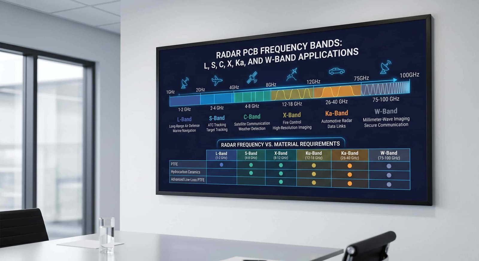
Radar System Types and Frequency Band Requirements
Different radar applications operate at different frequency bands, each with different PCB material and manufacturing requirements. Understanding the frequency band and application type is the first step in specifying the correct PCB.
L-Band and S-Band Radar (1–4 GHz)
L-band (1–2 GHz) and S-band (2–4 GHz) are used for long-range surveillance, air traffic control, weather radar, and ground-based early warning systems. At these frequencies, PCB insertion loss is less critical than at higher bands. Rogers RO4350B and RO4003C are suitable for most L-band and S-band radar PCB applications.
- Typical applications: early warning radar, ATC radar, weather surveillance, surface search radar
- PCB material: Rogers RO4350B or RO4003C — adequate Df at L/S-band frequencies
- Antenna size: relatively large — patch and array elements are 35–75 mm at L-band
- Power handling: L/S-band radar may use high power — PCB must handle RF power without dielectric heating
C-Band and X-Band Radar (4–12 GHz)
C-band (4–8 GHz) and X-band (8–12 GHz) are the most widely used bands for airborne radar, naval radar, missile seekers, and precision ground mapping. X-band is the dominant band for fire control radar and synthetic aperture radar (SAR). Rogers RO4350B covers most C-band applications. RO4003C and RO3003 are preferred for X-band where lower Df is needed.
- Typical applications: fire control radar, SAR, missile seeker, shipborne navigation radar, weather radar
- PCB material: Rogers RO4003C or RO3003 for X-band — lower Df than RO4350B
- Antenna dimensions: patch element approximately 8–15 mm at X-band
- Minimum line width: 3–5 mil for antenna feed lines at X-band on 0.508 mm substrate
Ku-Band and Ka-Band Radar (12–40 GHz)
Ku-band (12–18 GHz) and Ka-band (26.5–40 GHz) are used for high-resolution radar, missile guidance, satellite communication links, and millimeter-wave radar approaching the mmWave threshold. At Ka-band, insertion loss becomes a dominant concern and Rogers RO3003 or RT5880 are typically required.
- Typical applications: missile guidance seeker, high-resolution SAR, Ka-band satellite uplink, counter-drone radar
- PCB material: Rogers RO3003 or RT5880 — Df 0.0010 or lower required at Ka-band
- Antenna dimensions: patch element approximately 3–6 mm at Ka-band
- Minimum line width: 2.5–3 mil for antenna elements at Ka-band on 0.254 mm substrate
W-Band and mmWave Radar (75–110 GHz)
W-band (75–110 GHz) radar is used for high-resolution short-range imaging, precision approach systems, and next-generation defense sensing applications. At W-band, only ultra-low-loss materials such as Rogers RT5880 or specialized ceramics are suitable. Manufacturing tolerances must be extremely tight.
- Typical applications: precision approach radar, imaging radar, advanced ADAS (automotive), mmWave defense sensing
- PCB material: Rogers RT5880 (Dk 2.2, Df 0.0009) — only proven low-loss option at W-band
- Antenna dimensions: patch element approximately 1.0–1.5 mm at W-band
- Minimum line width: 2.5 mil or below — requires advanced capability manufacturing
AESA Phased Array Radar PCB Requirements
Active Electronically Scanned Array (AESA) radar represents the most demanding high frequency PCB application in defense electronics. An AESA radar replaces a mechanically rotating antenna with an array of individually controlled transmit/receive (T/R) elements that can steer the radar beam electronically without moving parts. This enables simultaneous multi-function radar operation, rapid beam steering, and high reliability with no moving mechanical parts.
T/R Module PCB
Each element in an AESA array has a dedicated T/R module that amplifies the transmit signal, receives the return signal, controls the phase shift for beam steering, and switches between transmit and receive modes. The T/R module PCB must handle RF power during transmit, maintain low noise figure during receive, and operate reliably across the full temperature range.
- Operating frequency: X-band (8–12 GHz) for most tactical AESA, Ka-band for next-generation systems
- PCB material: Rogers RO3003 or RT5880 for Ka-band T/R modules; RO4350B or RO4003C for X-band
- RF chip packages: GaAs or GaN MMIC in QFN or flip-chip format — thermal management critical
- Power handling: GaN T/R modules may dissipate 3–10W per element — thermal via arrays essential
- IPC Class 3 required — T/R module failure affects radar capability
Antenna Feed Network PCB
The corporate feed network distributes the transmit signal to all T/R modules and combines the received signals from all elements. Phase consistency across all feed paths is critical — any phase error between elements degrades beam quality and sidelobe performance.
- Phase matching: all feed paths from center to edge of array must be equal electrical length
- Insertion loss: lower loss in feed network means more power radiated — RT5880 preferred for large arrays
- Amplitude taper: corporate feed may use Wilkinson dividers or Butler matrix for amplitude tapering
- Isolation: each branch of the feed network must be isolated from adjacent branches
- Temperature stability: Dk temperature coefficient of the PCB material affects phase consistency over temperature
Beamforming PCB
In digital beamforming AESA systems, a separate beamforming board handles the digital phase and amplitude control signals for each T/R module. This board may combine high frequency analog and high-speed digital circuits on the same PCB — a hybrid design challenge requiring careful layer assignment and signal isolation.
- Hybrid stackup: Rogers or PTFE on RF layers, high-speed FR4 on digital layers
- Controlled impedance: 50Ω for RF, 50Ω/100Ω for high-speed digital signals
- Ground plane isolation between RF and digital layers
- Clock distribution: phase noise and jitter performance of clock distribution affects radar sensitivity
For hybrid stackup design, see FR4 + Rogers Hybrid PCB Stackup: When Should You Use It?. For multilayer considerations, see Multilayer High Frequency PCB: Layer Count, Stackup and Manufacturing Limits.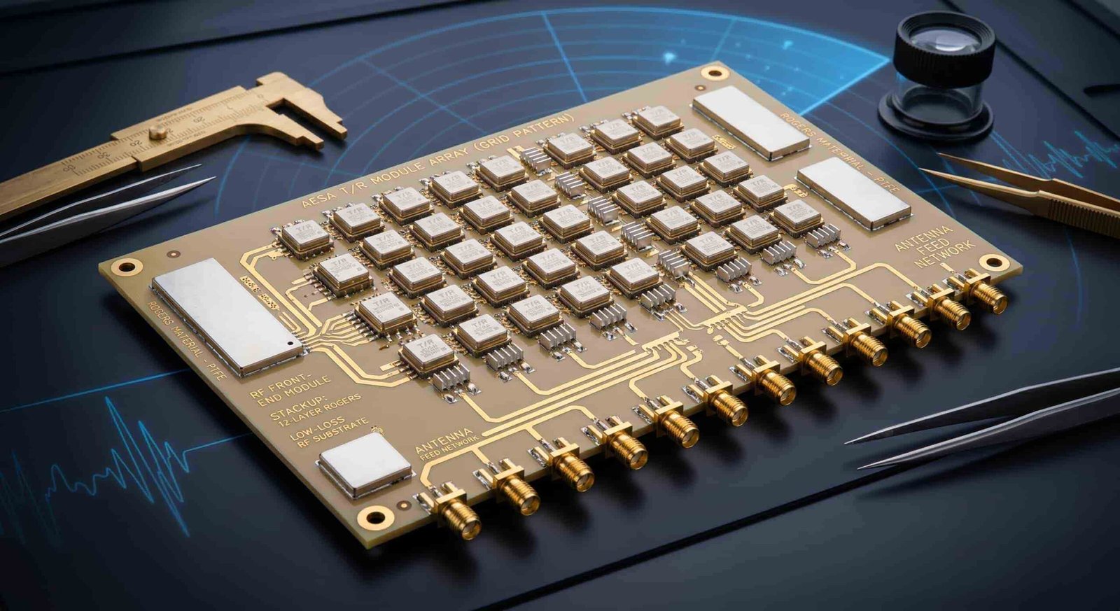
Electronic Warfare PCB Requirements
Electronic warfare (EW) systems include radar warning receivers (RWR), electronic countermeasures (ECM), electronic support measures (ESM), and jamming systems. EW PCB must operate across extremely wide frequency ranges — often 2–18 GHz or wider — with very low insertion loss and high dynamic range.
Wide Frequency Range Coverage
Unlike radar PCB which operates at a specific frequency band, EW PCB must perform consistently across a wide instantaneous bandwidth. This places unique demands on the PCB material — Dk must be stable across the entire frequency range, and the antenna or receiving element must be broadband.
- Typical EW frequency range: 2–18 GHz for tactical ESM/ECM, up to 40 GHz for advanced systems
- PCB material: Rogers RT5880 (Dk 2.2) preferred — lowest and most stable Dk across wide frequency range
- Rogers RO3003 (Dk 3.0) also used — lower Dk variation vs frequency than RO4350B
- Dk variation with frequency must be checked for the specific material and frequency range
Low Noise and High Dynamic Range
EW receivers must detect very weak signals in the presence of strong interferers. The PCB must minimize noise contribution, maintain good isolation between signal paths, and avoid passive intermodulation (PIM) products that could mask signals of interest.
- Surface finish: ENIG or ENEPIG — avoid immersion tin for high-dynamic-range EW receivers
- Ground plane continuity: no splits or slots under sensitive receiver signal paths
- Via fences: close-spaced via arrays between signal paths for isolation
- Solder mask: controlled coverage over RF traces to minimize dielectric variation
Low Probability of Intercept (LPI) Radar
LPI radar uses spread-spectrum and frequency-hopping waveforms to reduce the probability of detection and intercept by opposing EW systems. The PCB for LPI radar must support very wide instantaneous bandwidth and very low phase noise in the local oscillator distribution.
- PCB material: Rogers RT5880 — lowest Df minimizes signal degradation across wide bandwidth
- Local oscillator (LO) distribution: phase noise performance critical — short, low-loss LO paths
- Shielded enclosures: LO and sensitive circuits may require copper shielding cans soldered to PCB
- IPC Class 3: required for all operational LPI radar PCB
Material Selection for Defense Radar PCB by Frequency Band
Material selection for defense radar PCB depends on the operating frequency band, insertion loss budget, power handling requirement, and operating temperature range. The following guidance applies to the most common defense radar applications:
- L-band and S-band (1–4 GHz): Rogers RO4350B — adequate performance, cost-effective, standard multilayer process
- C-band (4–8 GHz): Rogers RO4003C or RO4350B — RO4003C preferred where lower Df is needed
- X-band (8–12 GHz): Rogers RO4003C or RO3003 — RO3003 for lowest loss requirements
- Ku-band (12–18 GHz): Rogers RO3003 — Df 0.0010 required at Ku-band frequencies
- Ka-band (26.5–40 GHz): Rogers RO3003 or RT5880 — RT5880 for lowest loss AESA and EW applications
- W-band (75–110 GHz): Rogers RT5880 only — no viable alternative at W-band for standard PCB
- Wide-band EW (2–18 GHz): Rogers RT5880 — most consistent Dk and lowest Df across full range
For detailed material properties, see Rogers PCB Material Selection Guide for RF and Microwave Applications and PTFE PCB Manufacturing Challenges and Process Considerations.
Thermal Management in Radar System PCB
Defense radar systems — particularly AESA T/R modules and high-power transmitter PCB — dissipate significant RF power that must be conducted away from active devices. The PCB thermal design must support the chip junction temperature limits across the full operating temperature range.
- GaN MMIC T/R modules: typical power dissipation 3–10W per element — very high thermal density
- Thermal via arrays under chip packages: 0.2–0.3 mm diameter, 0.6–0.8 mm pitch
- Copper coin inserts: for chips above 5W dissipation on standard PTFE substrates
- Internal copper planes: maximize copper fill on ground planes adjacent to power-dissipating layers
- Thermal interface material: between PCB and heat spreader or chassis — thermal resistance must be minimized
- Rogers RO3003 thermal conductivity: 0.5 W/m·K — adequate for moderate power density radar
- Rogers RT5880 thermal conductivity: 0.2 W/m·K — lower than RO3003 — thermal via density must be higher
Controlled Impedance for Radar System High Frequency PCB
Controlled impedance is a fundamental requirement for all radar system PCB. Every RF signal path — transmit chain, receive chain, LO distribution, antenna feed network — must be specified and verified to a controlled impedance value.
- Standard impedance tolerance: ±10% for most radar PCB signal paths
- Tighter tolerance: ±5% or absolute ±2–3Ω for phase-matched AESA feed networks
- Differential impedance: 100Ω for high-speed digital interfaces on hybrid boards
- Impedance coupon verification: TDR measurement of coupons on panel edge after production
- Stackup confirmation: actual Dk from material certificate used in impedance calculation — not nominal
- Temperature variation: Dk temperature coefficient of material must be included in worst-case impedance analysis
For controlled impedance background, see Why Controlled Impedance Matters in RF PCB Manufacturing. For stackup planning, see RF PCB Stackup Design: Key Factors Before Manufacturing.
Quality and Reliability Requirements for Defense Radar PCB
Defense radar PCB must meet the same high reliability standards as other aerospace and defense electronics. IPC Class 3 workmanship, full traceability, and qualification to applicable military standards are baseline requirements.
- IPC Class 3 workmanship: 25 µm average PTH copper plating, no annular ring breakout, 5% max void
- 100% electrical test: continuity and isolation for every board
- Impedance coupon verification: every production lot
- First article inspection: microsection, plating thickness, surface finish measurement
- Traceability: material certificates, laminate lot numbers, process records, serialization
- MIL-PRF-31032 or MIL-PRF-55110: applicable for boards required to meet US military specifications
- Conformal coating: commonly required for airborne and shipborne radar PCB
- Operating temperature: -55°C to +125°C standard for airborne; ground-based may specify wider
For IPC Class 3 details, see IPC Class 3 High Frequency PCB: What It Means for Aerospace and Defense Applications. For full aerospace and defense requirements, see High Frequency PCB for Aerospace and Defense: Material, Reliability and Manufacturing Requirements.
Information Needed for Radar System High Frequency PCB Quotation
To review feasibility and provide an accurate quotation for radar system high frequency PCB, the following information should be prepared:
- Gerber files (all layers) and NC drill files
- Complete PCB stackup with layer sequence, material, and dielectric thickness
- Radar system type and operating frequency band
- Material specification — Rogers grade or equivalent
- Layer count and board thickness
- Controlled impedance requirements — target, tolerance, and whether phase matching is required
- Via structure — through-hole, blind, buried, thermal vias
- Thermal requirements — chip power dissipation, thermal via density
- IPC Class requirement — Class 3 for defense radar
- Surface finish and thickness specification
- Traceability and documentation requirements
- Applicable military standards
- Quantity — prototype or production lot
- Working frequency range and application — EW, AESA, airborne, ground-based
For a complete quotation checklist, see What Files Are Needed for a High Frequency PCB Quotation?.
Conclusion
High frequency PCB for radar systems spans a wide range of applications — from L-band and S-band ground surveillance radar using Rogers RO4350B, to Ka-band and W-band AESA phased array systems requiring Rogers RO3003 or RT5880. Electronic warfare PCB demands the widest frequency coverage and lowest insertion loss, typically specifying Rogers RT5880 across the full 2–18 GHz or wider EW band.
AESA phased array radar PCB adds phase matching, thermal management for GaN T/R modules, and tight manufacturing tolerances to the standard high frequency PCB requirements. IPC Class 3 workmanship, full material and process traceability, and compliance with applicable military standards apply to all defense radar PCB. Early engineering review with a manufacturer experienced in defense radar PCB reduces design iteration and supports qualification and production.