Satellite communication systems span two categories of high frequency PCB: ground terminal electronics and space-borne electronics. Ground terminals — including VSAT terminals, military satellite uplink equipment, earth observation receive stations, and mobile satellite terminals — operate in demanding outdoor environments and must maintain RF performance across wide temperature ranges. Space-borne electronics on satellites and spacecraft face even more extreme requirements: vacuum, radiation, extreme thermal cycling, and zero maintenance access for the life of the mission.
Both categories rely on high frequency PCB materials and manufacturing processes that go beyond commercial RF PCB standards. Material selection, controlled impedance, layer registration, surface finish, outgassing properties, and radiation tolerance must all be considered together. The stakes of getting it wrong are high — a failed satellite cannot be repaired.
This guide covers the high frequency PCB requirements for satellite communication ground terminals and space-borne electronics, including frequency band requirements, material selection, space environment considerations, and manufacturing specifications.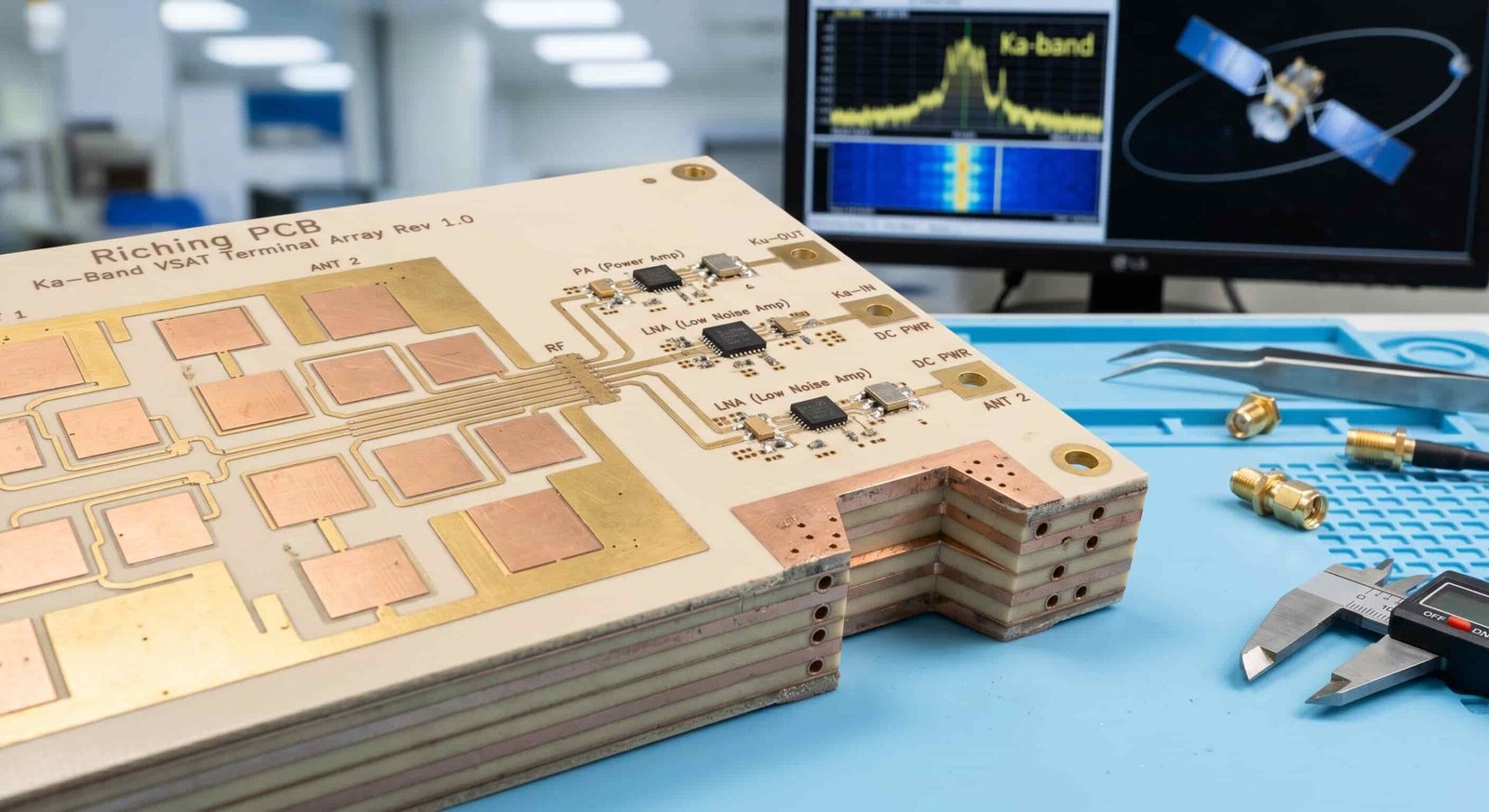
Quick Summary
Key point: Rogers RO3003 is the most widely used material for Ka-band satellite communication ground terminal PCB. Rogers RT5880 is used where the lowest insertion loss is required. Space-borne PCB adds outgassing (NASA ASTM E595 TML ≤ 1.0%), radiation hardness, and extreme thermal cycling requirements to standard aerospace PCB specifications. IPC Class 3 is the baseline for all satellite communication and space electronics PCB.
Ground terminal satellite PCB and space-borne satellite PCB share many common requirements but differ significantly in the additional space environment qualification that on-board electronics must meet. Understanding this distinction helps engineers specify the correct requirements and helps program managers set realistic schedules for qualification activities.
Satellite Communication Frequency Bands and PCB Requirements
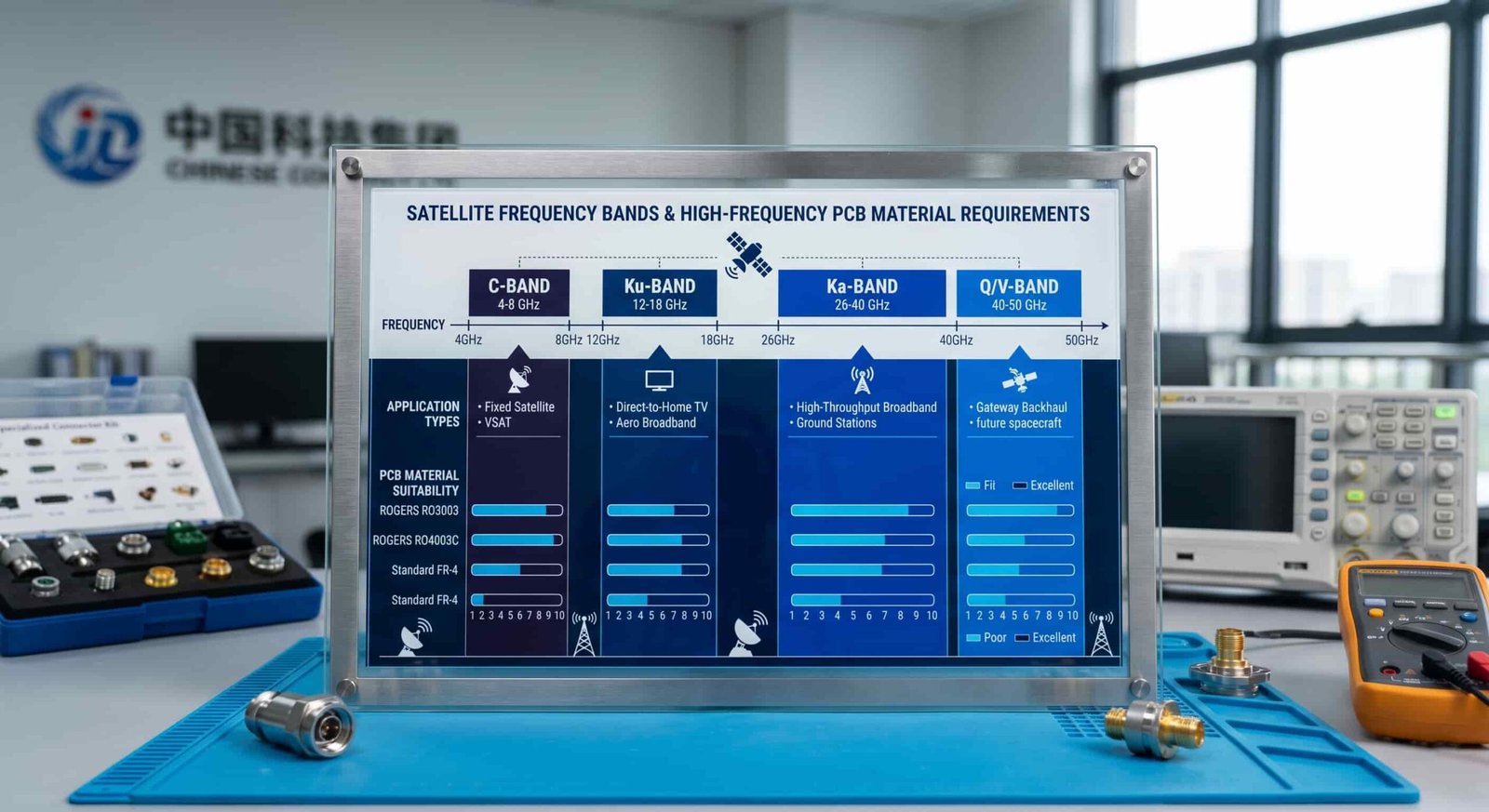
Satellite communication uses several frequency bands from C-band to Q/V-band, each with different PCB material and manufacturing requirements. The trend toward higher frequency bands — particularly Ka-band and Q/V-band — is driven by the need for higher data rates and wider bandwidth per transponder.
C-Band (3.7–7.25 GHz)
C-band is the oldest and most established satellite communication band. Its lower frequency means lower free-space path loss and better rain fade margin than higher bands, making it attractive for maritime and tropical applications. PCB requirements at C-band are moderate — Rogers RO4350B or RO4003C are suitable for most C-band ground terminal applications.
- Uplink: 5.85–7.075 GHz, Downlink: 3.7–4.2 GHz
- PCB material: Rogers RO4350B or RO4003C — adequate at C-band frequencies
- Applications: broadcast, maritime VSAT, military satellite communication
- Advantage over higher bands: better rain fade performance, suitable for tropical regions
Ku-Band (10.7–18 GHz)
Ku-band is the dominant band for commercial VSAT, direct broadcast satellite (DBS), and military protected satellite communication (MILSATCOM). At Ku-band, Rogers RO4003C provides good performance, but Rogers RO3003 is preferred for the lowest insertion loss feed networks and antenna arrays.
- Uplink: 13.75–14.5 GHz, Downlink: 10.7–12.75 GHz
- PCB material: Rogers RO4003C or RO3003 — RO3003 preferred for lowest loss
- Applications: VSAT, DBS, military Ku-band SATCOM terminals, aeronautical in-flight connectivity
- Rain fade: more susceptible than C-band — link budget must include rain fade margin
Ka-Band (26.5–40 GHz)
Ka-band is the fastest-growing satellite communication band, driven by high throughput satellite (HTS) systems offering multi-gigabit per second capacity. Ka-band PCB requires low-loss materials — Rogers RO3003 and RT5880 are the standard choices. Fine antenna trace dimensions at Ka-band demand tight manufacturing tolerances.
- Uplink: 27.5–31 GHz, Downlink: 17.7–21.2 GHz
- PCB material: Rogers RO3003 (Dk 3.0, Df 0.0010) or RT5880 (Dk 2.2, Df 0.0009)
- Applications: HTS ground terminals, military wideband SATCOM, LEO satellite user terminals
- Minimum line width: 2.5–3 mil for Ka-band antenna feed structures
- Rain fade: significant — Ka-band link budget must include substantial rain fade margin
Q/V-Band (37.5–75 GHz)
Q-band (37.5–42.5 GHz) and V-band (50–75 GHz) are emerging satellite bands for feeder links between gateway earth stations and satellites, offering very high capacity but requiring the lowest loss PCB materials available. Rogers RT5880 is the only standard PCB material suitable for Q/V-band applications.
- Applications: gateway feeder links, high capacity military satellite systems, next-generation HTS
- PCB material: Rogers RT5880 — only standard option at Q/V-band frequencies
- Manufacturing: minimum line width capability 2.5 mil or below required
- Rain fade: very severe — Q/V-band systems require adaptive coding and modulation
Satellite Communication Ground Terminal PCB Requirements
Ground terminal high frequency PCB includes the RF front-end, antenna feed network, low noise amplifier (LNA), power amplifier (PA), frequency conversion chain, and signal processing circuits. Each has different PCB requirements.
Antenna Feed Network PCB
The antenna feed network distributes the transmit signal to all antenna elements and combines received signals from all elements. For phased array terminals — increasingly common in Ka-band and Q/V-band military SATCOM — phase consistency across all feed paths is critical for beam pointing accuracy.
- Material: Rogers RO3003 or RT5880 for Ka-band — lowest Dk and Df minimize insertion loss and phase error
- Phase matching: equal electrical length for all feed paths from center to edge of array
- Impedance: 50Ω for single-ended feed lines, controlled to ±10% standard
- Surface finish: ENIG — flat surface ensures consistent RF pad performance
LNA PCB
The low noise amplifier is the most noise-sensitive part of the receive chain. Any resistive loss in the PCB between the antenna and the LNA input adds directly to the system noise figure. The shortest, lowest-loss path from antenna to LNA input is always preferred.
- Material: Rogers RO3003 or RT5880 — lowest Df minimizes noise contribution from PCB traces
- PCB trace length: minimize distance between antenna feed and LNA input
- Grounding: solid, continuous ground plane under LNA input circuit
- Surface finish: ENIG — gold surface maintains consistent contact resistance over time
Power Amplifier PCB
The power amplifier transmit chain must handle significant RF power — typically 10–100W for ground terminals, higher for gateway stations. Thermal management is critical: GaAs or GaN PA chips dissipate substantial heat that must be conducted through the PCB to a heat sink or chassis.
- Material: Rogers RO3003 for Ka-band PA PCB — CTE match to copper reduces solder joint stress
- Thermal vias: dense array under PA chip package — 0.2–0.3 mm diameter, 0.5–0.8 mm pitch
- Copper planes: maximize copper fill on ground layers adjacent to PA for heat spreading
- Power handling: PCB dielectric must not heat significantly under rated RF power
Space-Borne High Frequency PCB: Additional Requirements
Space-borne PCB on satellites and spacecraft faces requirements that go beyond those for ground terminal electronics. The space environment imposes constraints that directly affect material selection, manufacturing process, and qualification testing.
Vacuum Outgassing
In the vacuum of space, materials that contain trapped solvents, moisture, or volatile compounds will outgas — releasing these materials into the vacuum. Outgassing can contaminate sensitive optical surfaces, solar cells, and thermal control surfaces on the spacecraft. All PCB materials and surface finishes used in space-borne electronics must meet outgassing requirements.
- NASA standard: ASTM E595 — Total Mass Loss (TML) ≤ 1.0%, Collected Volatile Condensable Materials (CVCM) ≤ 0.10%
- Rogers RT5880 ASTM E595: TML typically 0.02–0.05%, CVCM <0.01% — excellent outgassing performance
- Rogers RO3003 ASTM E595: similar low outgassing performance
- Solder mask: must be space-qualified — standard commercial solder mask may not meet outgassing requirements
- Surface finish: ENIG and ENEPIG are generally compatible with space outgassing requirements
- Conformal coating: not typically used on space PCB — coating must be space-qualified if required
Radiation Effects
Space-borne electronics are exposed to ionizing radiation from the Van Allen belts, solar particle events, and galactic cosmic rays. The radiation dose depends on the orbit (LEO, MEO, GEO) and the mission duration. PCB laminate materials are generally radiation-tolerant, but the organic resin components can degrade at very high doses.
- Low Earth Orbit (LEO): total ionizing dose typically 10–100 krad over 5-year mission
- Geostationary Orbit (GEO): total ionizing dose typically 100 krad to 1 Mrad over 15-year mission
- Rogers PTFE materials: PTFE base is inherently radiation-tolerant — suitable for most LEO and GEO missions
- Radiation hardness testing: TID (Total Ionizing Dose) testing per MIL-STD-883 Method 1019
- Single event effects: not typically a concern for PCB laminate — concern for active devices
Note: PCB laminate radiation tolerance is generally not the limiting factor for space electronics. Active components — transistors, amplifiers, and digital ICs — typically set the radiation hardness requirement for the assembly. The PCB material must be demonstrated to maintain its dielectric properties and structural integrity at the required total dose level.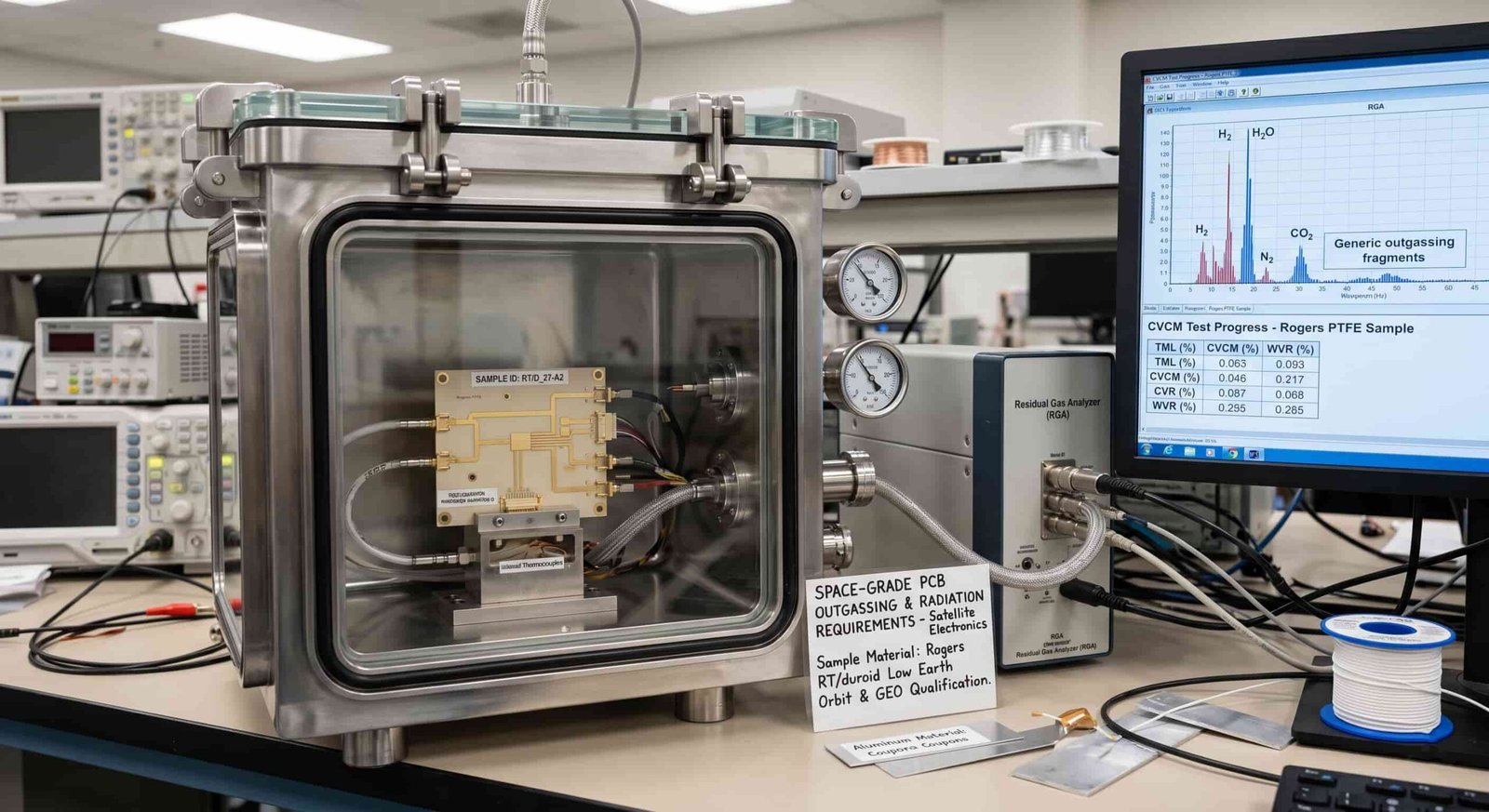
Extreme Thermal Cycling in Space
Satellites in low earth orbit experience a thermal cycle every orbit — approximately every 90 minutes for a 400 km orbit. Over a 5-year mission, this amounts to approximately 30,000 thermal cycles. The temperature excursion depends on the thermal control design but may be -100°C to +100°C or wider for uncontrolled surfaces.
- LEO thermal cycle: approximately 16 cycles per day, 5,840 cycles per year
- GEO thermal cycle: approximately 2 cycles per day during eclipse season
- Space-borne PCB must survive 30,000+ cycles for LEO missions without via barrel failure
- PTFE materials with high z-axis CTE (Rogers RT5880) require careful via design for extreme thermal cycling
- Copper-filled vias and blind vias significantly improve thermal cycling reliability
- Thermal cycling qualification: must cover the full mission life, often with acceleration factor
Single Point of Failure — No Repair
The most fundamental difference between space-borne and ground-based electronics is that space-borne systems cannot be repaired after launch. A via barrel crack or delamination discovered on a satellite in orbit cannot be fixed. This drives the very high reliability requirements and qualification standards applied to space PCB.
- No in-service repair: all failure modes must be addressed before launch
- Redundancy: critical signal paths often have redundant routing or component redundancy
- Lot traceability: every component and PCB must be traceable to manufacturing lot for failure analysis if needed
- Part screening: active components screened for early failures before assembly
- Workmanship: typically IPC Class 3 or higher — some programs define their own standards above Class 3
Material Selection for Satellite Communication PCB
Material selection for satellite communication PCB depends on whether the application is a ground terminal or space-borne system, the operating frequency band, and the thermal and radiation environment.
Ground Terminal PCB Material Selection
- C-band ground terminal: Rogers RO4350B or RO4003C — cost-effective, adequate performance
- Ku-band ground terminal: Rogers RO4003C or RO3003 — RO3003 preferred for lowest loss
- Ka-band ground terminal: Rogers RO3003 — best balance of loss, Dk stability, and CTE for Ka-band
- Ka-band lowest loss terminal: Rogers RT5880 — for applications where every tenth of a dB matters
- Q/V-band gateway: Rogers RT5880 — only viable standard option at Q/V-band
Space-Borne PCB Material Selection
- Space-borne Ku-band and Ka-band: Rogers RT5880 — best outgassing performance, PTFE radiation tolerance
- Space-borne C-band: Rogers RO4350B or RO3003 — confirmed outgassing qualification required
- All space-borne PCB: outgassing data (ASTM E595) must be confirmed from the manufacturer before specification
- Solder mask: space-qualified solder mask required — standard commercial products must be tested
For Rogers material properties and selection guidance, see Rogers PCB Material Selection Guide for RF and Microwave Applications. For PTFE process requirements, see PTFE PCB Manufacturing Challenges and Process Considerations.
Controlled Impedance for Satellite Communication PCB
Controlled impedance is a standard requirement for all satellite communication PCB. The impedance specification must be maintained across the full operating temperature range, which may be -55°C to +85°C for ground terminals and -100°C to +100°C for space-borne systems.
- Standard impedance tolerance: ±10% for ground terminal satellite PCB
- Tighter tolerance: ±5% for phase-matched phased array feed networks
- Temperature variation: Dk temperature coefficient must be included in worst-case impedance analysis
- Impedance coupon verification: TDR measurement of coupons after production — every lot
- Stackup confirmation: actual Dk from material certificate used in calculation
- Space-borne: impedance must be verified to remain within specification across full on-orbit temperature range
For controlled impedance background, see Why Controlled Impedance Matters in RF PCB Manufacturing. For stackup design, see RF PCB Stackup Design: Key Factors Before Manufacturing.
Quality Requirements for Satellite Communication PCB
IPC Class 3 is the baseline quality standard for satellite communication PCB. Space-borne programs may define additional requirements above Class 3 based on mission criticality and the consequences of failure.
- IPC Class 3: 25 µm average PTH copper plating, no annular ring breakout, 5% max void, 100% electrical test
- First article inspection: microsection, plating thickness, surface finish measurement, impedance verification
- Traceability: material certificates, laminate lot numbers, process records, board serialization
- Ground terminal: MIL-PRF-31032 or equivalent may be specified for military SATCOM programs
- Space-borne: ECSS-Q-ST-70-11 (European) or NASA workmanship standards for space programs
- Record retention: typically the satellite design life plus 5 years — 10–20 years for GEO programs
For IPC Class 3 requirements in detail, see IPC Class 3 High Frequency PCB: What It Means for Aerospace and Defense Applications. For full aerospace and defense requirements, see High Frequency PCB for Aerospace and Defense: Material, Reliability and Manufacturing Requirements.
Information Needed for Satellite Communication PCB Quotation
To review feasibility and provide an accurate quotation for satellite communication high frequency PCB, the following information should be prepared:
- Gerber files (all layers) and NC drill files
- Complete PCB stackup with material specification, layer sequence, and copper weight
- Application: ground terminal or space-borne
- Frequency band: C-band, Ku-band, Ka-band, Q/V-band, or other
- Material specification — Rogers grade or equivalent
- Layer count and board thickness
- Controlled impedance requirements — target, tolerance, temperature range
- Via structure — through-hole, blind, buried, copper-filled
- Outgassing requirement — ASTM E595 TML and CVCM limits if space-borne
- Radiation requirement — total dose, orbit, mission duration if space-borne
- Thermal cycling requirement — temperature range and number of cycles
- IPC Class requirement — Class 3 or above
- Surface finish and thickness specification
- Traceability and documentation requirements
- Applicable standards — MIL-PRF-31032, ECSS, NASA, or other
- Quantity — prototype, engineering model, or flight unit
- Working frequency and application background
For a complete file checklist, see What Files Are Needed for a High Frequency PCB Quotation?.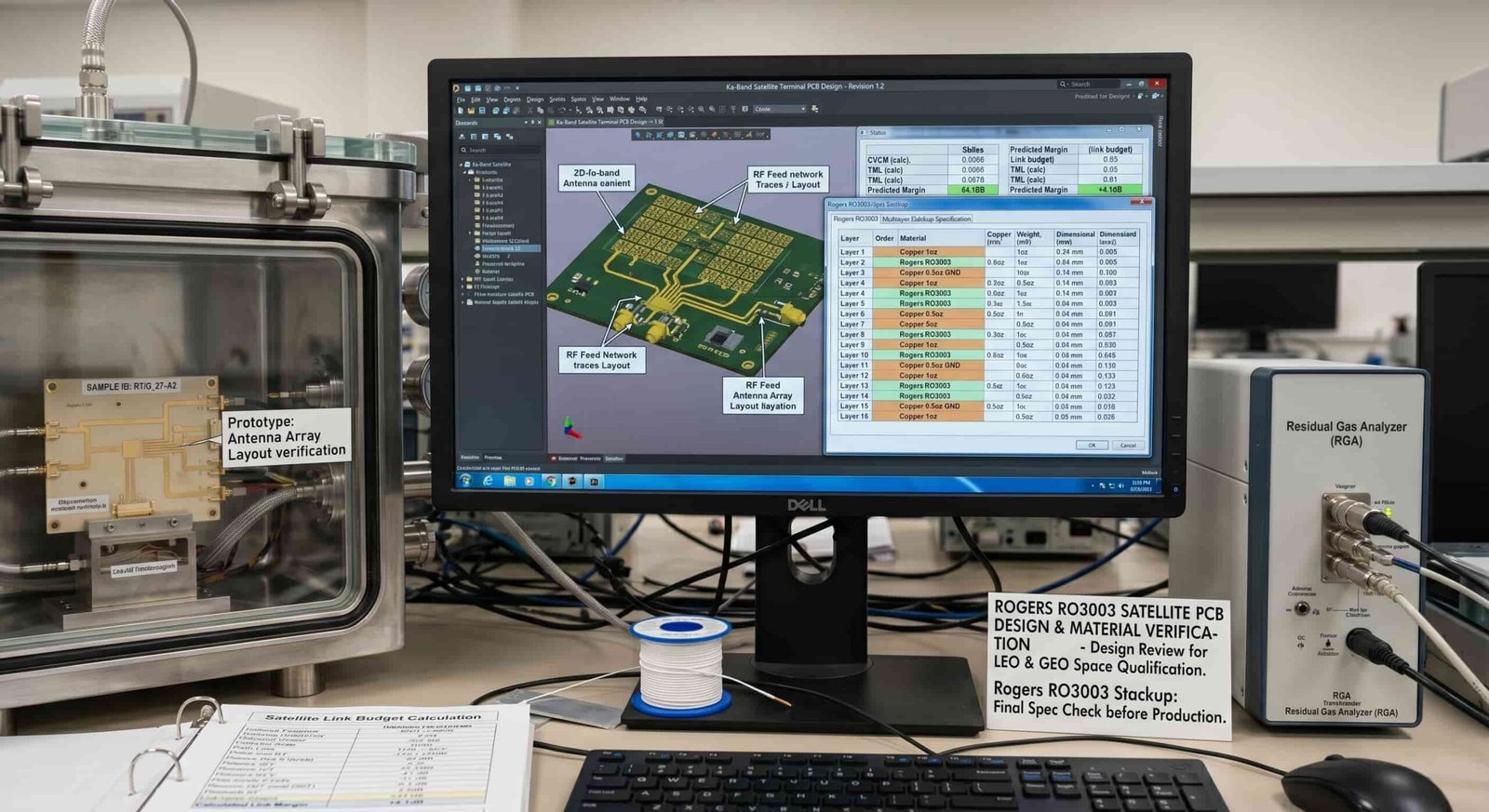
Conclusion
High frequency PCB for satellite communication spans ground terminal equipment and space-borne electronics. Ground terminals operating at Ku-band and Ka-band rely on Rogers RO3003 and RT5880 for low-loss antenna feed networks, LNA PCB, and phased array terminals. Space-borne electronics add outgassing qualification to ASTM E595, radiation tolerance verification, and extreme thermal cycling reliability to the standard aerospace PCB requirements.
IPC Class 3 workmanship, full material traceability, impedance coupon verification, and first article inspection are baseline requirements for all satellite communication high frequency PCB. Space-borne programs require additional qualification steps — outgassing testing, radiation testing, and extended thermal cycling — that must be planned into the program schedule from the beginning. Early engagement with an RF PCB manufacturer experienced in satellite and space electronics significantly reduces qualification risk.