Wireless infrastructure PCB is used in equipment that supports RF transmission, signal routing, antenna connection, wireless coverage, and communication network hardware. These boards may appear in base station modules, remote radio units, small cells, repeaters, antenna systems, RF front-end boards, and microwave communication equipment.
For this type of PCB, manufacturing review cannot stop at layer count and board size. Material selection, stackup, impedance, grounding, connector launch, plated through holes, thermal behavior, surface finish, and production repeatability all affect performance.
For buyers, the goal is not only to receive a working prototype. Wireless infrastructure equipment often moves into repeated production, so the PCB must be manufacturable, testable, and consistent across batches.
Quick Summary
Wireless infrastructure PCBs are used in base station equipment, remote radio units, small cells, RF modules, antenna systems, repeaters, and microwave communication hardware.
These boards often require controlled impedance, low-loss or high frequency materials, stable ground reference, reliable RF connectors, strong plated through holes, and good thermal design.
The main risks include impedance shift, signal loss, weak connector launch, poor via grounding, material substitution, thermal stress, and prototype-to-batch inconsistency.
Before quotation, buyers should provide Gerber files, drill files, stackup, material requirement, working frequency, impedance details, copper thickness, surface finish, connector information, quantity, and application background.
Where Wireless Infrastructure PCBs Are Used
Wireless infrastructure covers many types of communication equipment. Some boards carry RF signals directly, while others combine RF, digital, power, and control circuits.
Common applications include:
Remote radio units
Small cell equipment
Repeater systems
Antenna interface boards
Microwave communication modules
Wireless backhaul equipment
RF front-end circuits
Power amplifier boards
Telecom test and monitoring devices
A board used near an antenna path may have different material and impedance requirements from a control board inside the same system. This is why buyers should explain the board function when sending files for quotation.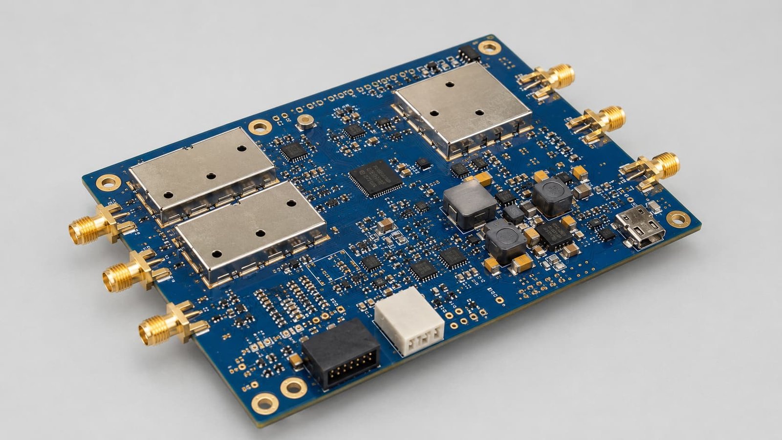
Material Selection
Material selection depends on frequency, signal loss target, stackup, and production cost.
Some non-critical control areas may use FR4. RF and microwave signal paths may require Rogers materials, PTFE, Taconic, F4B, or hybrid stackups. The final choice should match the design requirement instead of being selected only by material price.
The material review should include:
Working frequency
Dk and Df values
Dielectric thickness
Copper thickness
Board thickness
Copper roughness
Thermal behavior
Material availability
Batch repeatability
Wireless infrastructure products often require stable supply. A material that works for one prototype may not be ideal if it is difficult to source for later production.
Stackup and Controlled Impedance
Wireless infrastructure PCBs often include controlled impedance traces for RF paths, antenna feed lines, connector transitions, filters, and high frequency signal routing.
A proper stackup review should confirm:
Layer count
Material type
Dielectric thickness
Copper thickness
RF signal layer
Ground reference plane
Power layer
Final board thickness
Controlled impedance target
Via structure
Surface finish
The impedance calculation should be based on the real production stackup. If dielectric thickness or copper thickness changes during production, the final impedance may shift.
In wireless infrastructure equipment, this can affect RF performance, matching, signal transmission, and repeatability between boards.
RF Connectors and Cable Interfaces
RF connector areas are key risk points.
Wireless infrastructure boards may use SMA, SMP, board-to-board RF connectors, coaxial cable interfaces, edge launch structures, or custom RF connections. These areas need both electrical and mechanical review.
The review should include:
Connector footprint
Pad-to-trace transition
Ground via placement
Reference plane continuity
Mounting hole tolerance
Copper clearance
Surface finish
Cable stress
Assembly method
A strong RF trace can still fail if the connector launch is weak. Poor ground via placement or a broken reference plane near the connector can create reflection and unstable RF behavior.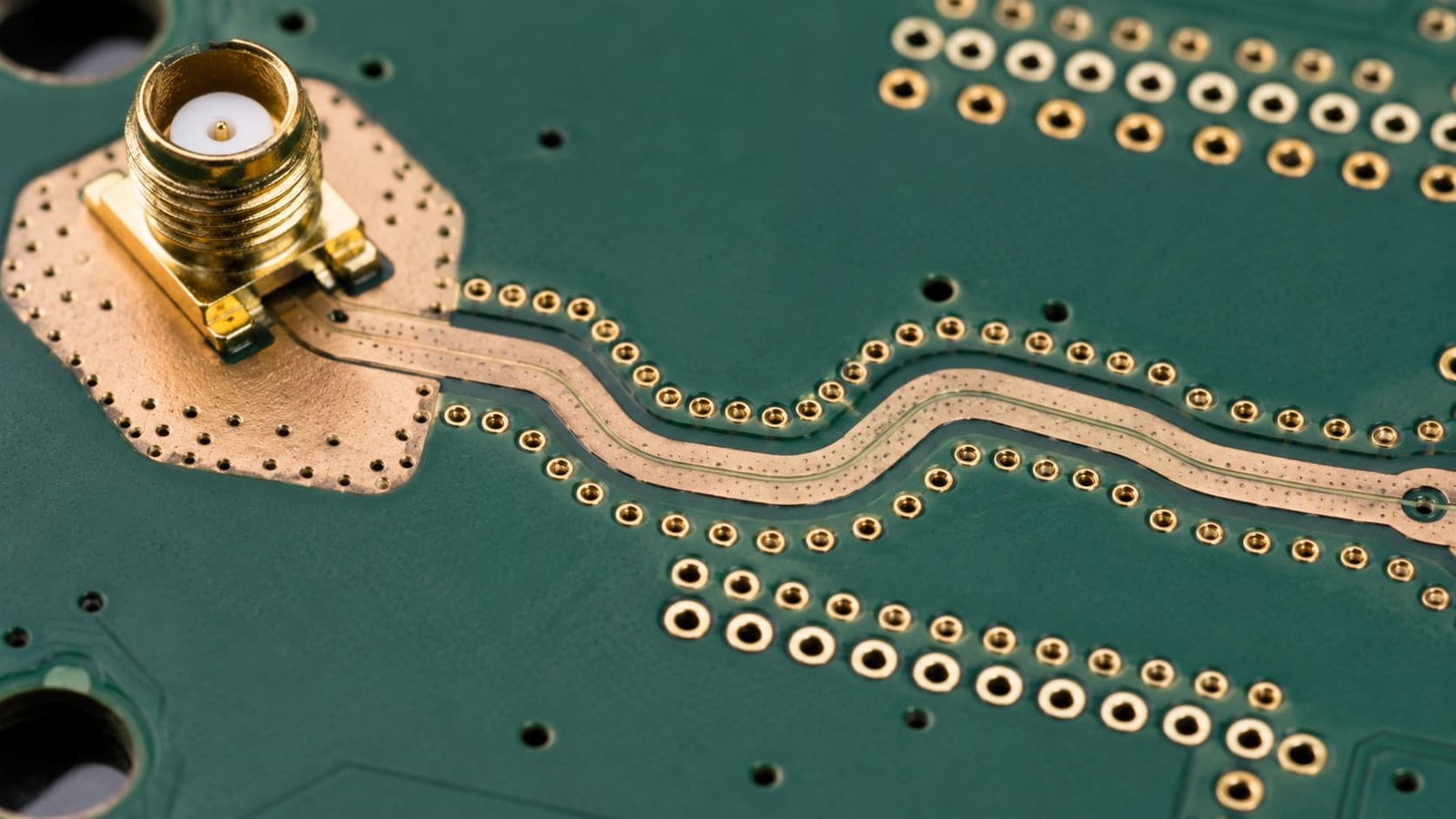
Grounding and Via Design
Grounding is central to wireless infrastructure PCB performance.
A clean ground reference helps control RF return paths, reduce noise, improve shielding, and support stable impedance. Via stitching is often used around RF paths, connectors, shielding areas, and board edges.
Important via points include:
Ground via spacing
Via fence design
Signal via size
Via stub length
Connector grounding vias
Plated through-hole quality
Anti-pad clearance
Layer transition path
For multilayer RF boards, via transitions should be reviewed before manufacturing. If the board has microwave paths, uncontrolled via stubs may affect performance.
Thermal and Mechanical Reliability
Wireless infrastructure equipment may work in cabinets, outdoor enclosures, power modules, or high-density communication systems. Heat and mechanical stress should be reviewed early.
Thermal and mechanical review may include:
Copper thickness
Thermal vias
Heat sink mounting holes
Power component areas
Large copper balance
Board thickness
Plated through-hole reliability
Connector mechanical strength
Enclosure mounting points
Thermal design is not only about component temperature. It can also affect material stability, solder joint reliability, copper adhesion, and long-term board performance.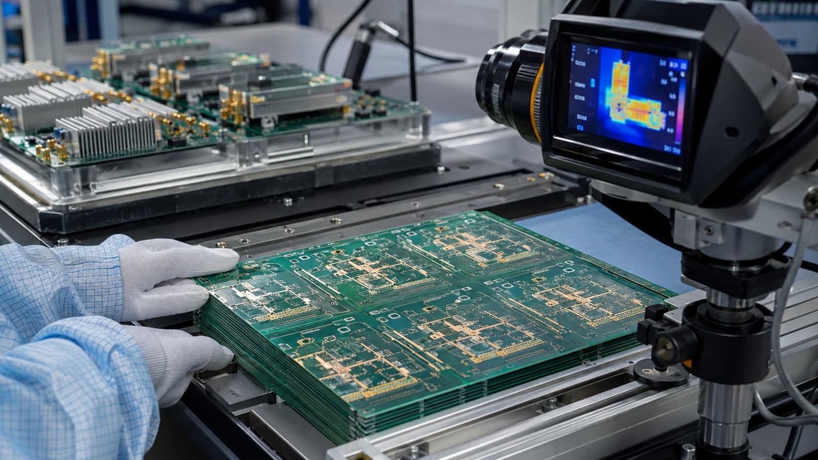
Surface Finish Selection
Surface finish should match assembly, connector areas, storage, and reliability requirements.
Common options include:
ENIG
Immersion silver
OSP
Lead-free HASL
Hard gold for contact areas
Customer-specified finishes
ENIG is commonly used because it provides a flat surface and stable solderability. Hard gold may be needed in contact or repeated mating areas. Immersion silver may be reviewed for some RF-sensitive applications.
The finish should not be selected only by habit. It should match the RF requirement, connector structure, assembly process, and operating condition.
Manufacturing Review Before Production
Wireless infrastructure PCB projects should be reviewed before fabrication.
A practical review includes:
Material availability
Stackup feasibility
Drilling tolerance
Plated through-hole reliability
Trace width tolerance
Connector footprint
Ground via structure
Thermal via design
Surface finish
Panelization
Inspection method
Prototype and batch plan
If the board will be produced repeatedly, the manufacturer should confirm whether the material, stackup, and process can be maintained for future orders.
What Buyers Should Provide for Quotation
A complete quotation package helps reduce engineering delay and material risk.
Buyers should prepare:
Gerber files
Drill files
PCB stackup
Material requirement
Working frequency
Controlled impedance table
Board thickness
Copper thickness
Surface finish
Connector type
Quantity
Prototype or batch plan
Application background
Thermal or mechanical requirements
If the buyer is unsure about the material, the working frequency and board function are very helpful. The manufacturer can then review whether FR4, Rogers, PTFE, Taconic, F4B, or a hybrid structure is more practical.
Common Mistakes to Avoid
Common mistakes include:
Treating RF and control sections the same
Choosing material only by price
Sending Gerber files without stackup
Ignoring connector launch areas
Using too few ground vias
Changing material after prototype
No controlled impedance table
Ignoring heat sink and mounting areas
Selecting surface finish by habit
Not checking batch repeatability
These issues may not appear during visual inspection. They often show up during RF testing, assembly, environmental stress, or repeat production.
Conclusion
Wireless infrastructure PCB manufacturing requires careful review of material, stackup, controlled impedance, RF connectors, grounding, vias, thermal design, surface finish, and production consistency.
For base stations, remote radio units, small cells, antenna systems, repeaters, and microwave communication equipment, the PCB is part of the RF system. It should not be treated like a standard circuit carrier.
The best results come when buyers provide complete files, working frequency, impedance requirements, material preferences, connector details, and application background before production begins.