Phased Array Antenna PCB: Manufacturing Requirements and Production Review
Phased array antenna PCB is used when multiple antenna elements must work together with controlled signal timing, stable RF paths, and repeatable manufacturing accuracy. These boards are common in radar electronics, satellite communication, 5G systems, wireless infrastructure, aerospace RF modules, and advanced antenna equipment.
Unlike a simple antenna board, a phased array antenna PCB often has repeated antenna elements, RF feed networks, ground structures, via fences, connector areas, and strict layout symmetry. Small differences in material thickness, copper pattern, impedance, or production tolerance may affect phase consistency and final antenna performance.
For buyers, this type of PCB should not be treated as a standard high-frequency board with more copper patterns. The material, stackup, impedance, layout, drilling, surface finish, and production repeatability should all be reviewed before fabrication.
Quick Summary
- Phased array antenna PCBsare used in radar systems, satellite communication, 5G antenna modules, aerospace RF equipment, wireless infrastructure, and high-frequency antenna products.
- These boards typically require stable high-frequency materials, controlled impedance, accurate RF feed networks, tight copper pattern control, reliable grounding vias, and strong production consistency.
- The main risks include impedance shift, phase mismatch, copper pattern deviation, poor via grounding, material substitution, connector launch mismatch, and prototype-to-batch inconsistency.
- Before quotation, buyers should provide Gerber files, drill files, stackup, material requirement, working frequency, impedance details, copper thickness, surface finish, quantity, and application background.
Where Phased Array Antenna PCBs Are Used
Phased array antenna PCBs are used when an antenna system needs beam control, directional performance, or multiple radiating elements working together.
Typical applications include:
- Radar antenna modules
- Satellite communication antennas
- 5G antenna systems
- Wireless infrastructure
- Aerospace RF equipment
- Microwave communication systems
- Automotive radar-related boards
- RF sensing equipment
- Defense and industrial RF systems
- High-frequency test platforms
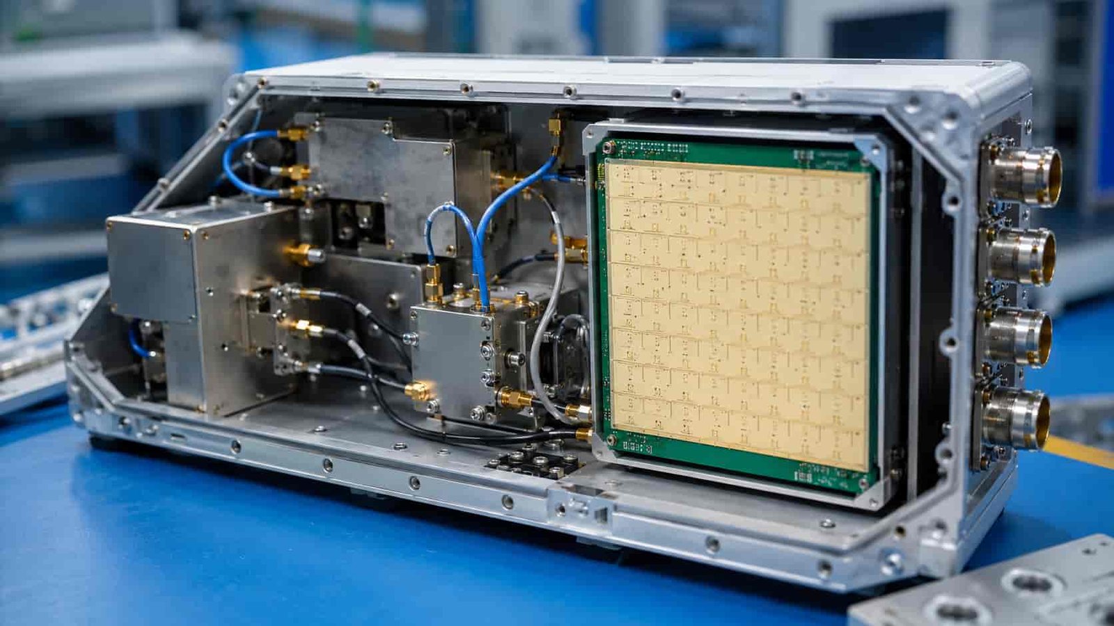
The board may include antenna elements, power dividers, phase control sections, RF connectors, matching networks, and ground vias. The manufacturer must understand which parts of the board are RF-sensitive before production starts.
Material Selection
Material selection is one of the first and most important decisions in phased array antenna PCB manufacturing.
The material affects Dk, Df, impedance, signal loss, wavelength, antenna element size, and phase behavior. For this reason, standard FR4 is generally not sufficient for sensitive phased array antenna applications.
Common material options include:
- Rogers materials
- PTFE laminates
- Taconic materials
- F4B materials
- Low-loss microwave laminates
- Hybrid stackups for mixed RF and control sections
The material review should include:
- Working frequency
- Dk and Df values
- Dk tolerance
- Dielectric thickness
- Copper thickness
- Copper roughness
- Board thickness
- Material availability
- Batch repeatability
In phased array designs, material consistency matters because repeated antenna elements should behave uniformly across the board and across production batches. Even small Dk variation between material lots can affect phase consistency.
Stackup and Antenna Element Control
The stackup is part of the antenna design, not just a mechanical specification.
A complete stackup review should define:
- Layer count
- Material type
- Dielectric thickness
- Copper thickness
- Antenna layer
- RF feed layer
- Ground reference plane
- Power or control layers
- Final board thickness
- Controlled impedance target and tolerance
- Via structure
- Surface finish
If dielectric thickness changes, antenna resonant behavior may shift. If copper thickness changes, trace width and impedance may deviate. If the ground reference is inconsistent, feed network performance may become unpredictable.
For phased array antenna PCBs, stackup changes should not be made after layout is completed without a full RF review.
RF Feed Network and Phase Consistency
The RF feed network is one of the most sensitive parts of a phased array antenna PCB.
It may include power dividers, controlled impedance traces, matching structures, branch lines, phase paths, and connector transitions. If one path differs slightly from another, the antenna system may not perform as expected.
The review should include:
- Trace width and tolerance
- Trace length matching
- Trace spacing
- Copper etching tolerance
- Power divider symmetry
- Ground reference continuity
- Via transition consistency
- Connector launch structure
- Antenna element spacing
- Impedance tolerance
For this type of PCB, manufacturing accuracy is not only about passing electrical continuity testing. It is about keeping repeated RF paths as consistent as the design requires. This is where high-frequency PCB process control directly affects antenna system performance.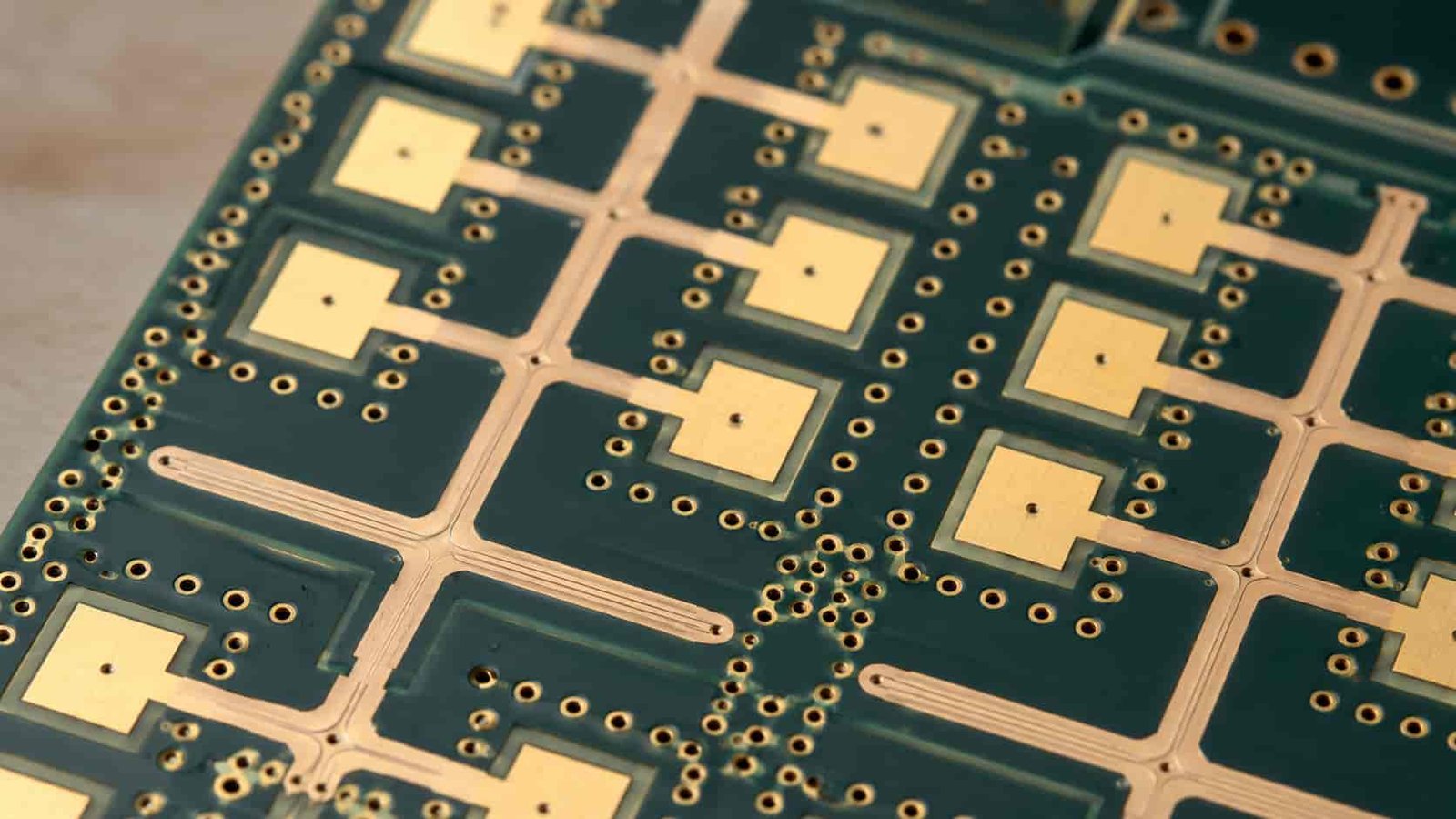
Controlled Impedance
Controlled impedance is typically required in phased array antenna PCB projects, particularly for feed lines, power dividers, and connector transitions.
The impedance depends on:
- Material Dk
- Dielectric thickness
- Trace width
- Copper thickness
- Reference plane
- Solder mask condition
- Etching tolerance
- Final production stackup
The manufacturer should calculate impedance based on the real production stackup. If the buyer provides only Gerber files without impedance information, the quotation may overlook a critical RF requirement.
For antenna feed lines and microwave paths, impedance should be confirmed before fabrication. Once the board is finished, impedance problems typically require redesign or a new production run.
Vias, Grounding, and Via Fences
Vias are widely used in phased array antenna PCBs for grounding, shielding, signal transition, and RF isolation.
Important via design points include:
- Ground via spacing
- Via fence design and pitch
- Signal via size
- Via stub length
- Antenna element isolation
- Connector grounding vias
- Plated through-hole reliability
- Anti-pad clearance
- Layer transition path
Grounding should be consistent around repeated antenna elements and RF feed structures. If some areas have stronger ground connection than others, the antenna array may show uneven radiation performance.
Via fences can improve isolation between elements, but their spacing and distance from RF traces must be reviewed carefully. Incorrect placement may affect impedance or antenna resonance.
Connector Areas and Mechanical Fit
Phased array antenna PCBs may connect to RF cables, board-to-board connectors, module housings, or metal antenna structures.
Connector areas should be reviewed for:
- Connector footprint accuracy
- Pad-to-trace transition geometry
- Ground via placement
- Reference plane continuity
- Mounting hole accuracy
- Board outline tolerance
- Enclosure fit
- Surface finish compatibility
- Assembly method
Mechanical fit is especially important when the PCB becomes part of an antenna module. If the board outline, mounting holes, or connector positions are not controlled, the assembly process itself may affect RF performance.
Surface Finish
Surface finish should match soldering requirements, connector areas, antenna surfaces, storage conditions, and assembly process.
Common options include:
- ENIG
- Immersion silver
- OSP
- Lead-free HASL
- Hard gold for repeated contact areas
- Customer-specified finishes
ENIG is widely used because it provides a flat, solderable surface. Immersion silver may be reviewed for RF-sensitive exposed areas where surface conductivity matters. Hard gold may be required for repeated-contact or connector pads.
The finish should be selected based on RF requirement and assembly condition, not by standard purchasing habit alone.
Manufacturing and Inspection Review
Phased array antenna PCB manufacturing requires careful process control at every stage.
The review should include:
- Material availability and lot consistency
- Stackup feasibility
- Controlled impedance verification
- Trace width tolerance
- Copper etching accuracy
- Drilling tolerance
- Plated through-hole reliability
- Via fence structure
- Surface finish
- Board outline tolerance
- Panelization
- Inspection method
- Prototype and batch plan
Repeated antenna patterns should be inspected carefully. A small pattern variation across the panel may affect antenna uniformity even when the board passes standard electrical testing.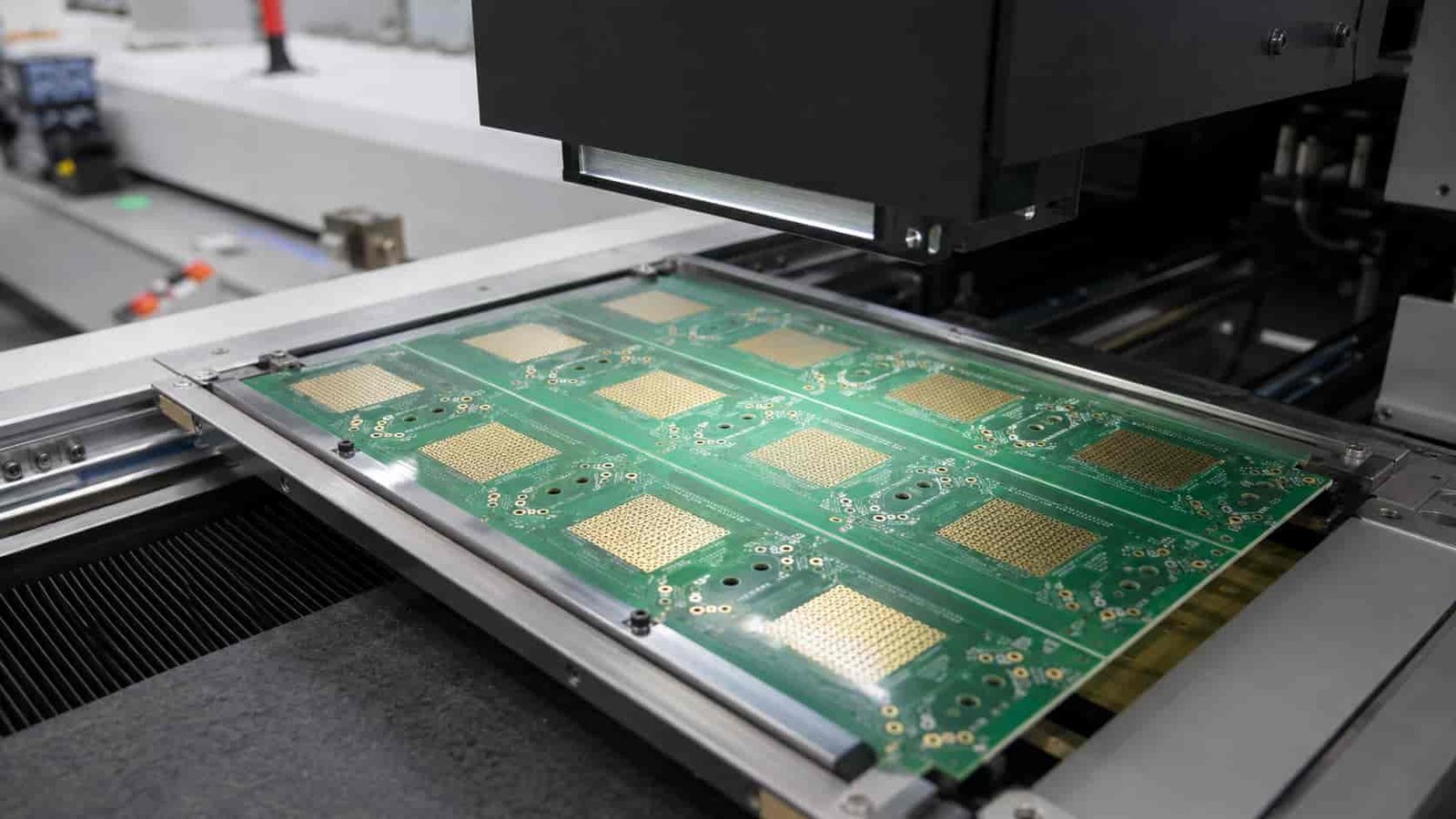
Prototype-to-Batch Consistency
A phased array antenna PCB prototype may pass initial testing, but batch production can still introduce performance variation.
Batch differences may come from:
- Material lot variation
- Dielectric thickness change
- Copper thickness variation
- Etching tolerance shift
- Different surface finish
- Panelization changes
- Connector assembly variation
- Different inspection criteria
- Missing impedance test requirement
Buyers should confirm whether the approved stackup, material, copper thickness, and production process can be consistently repeated for future orders.
For antenna systems, repeatability is often more important than a single successful prototype.
What Buyers Should Provide for Quotation
A complete quotation request helps the manufacturer identify RF risk before pricing.
Buyers should prepare:
- Gerber files
- Drill files
- PCB stackup
- Material requirement
- Working frequency
- Controlled impedance table
- Board thickness
- Copper thickness
- Surface finish
- Connector information
- Quantity
- Prototype or batch plan
- Application background
- Special antenna or RF requirements
If the material is not yet fixed, working frequency, antenna structure, and application background are especially useful. The manufacturer can then review whether Rogers, PTFE, Taconic, F4B, or a hybrid stackup is more appropriate for the application.
Common Mistakes to Avoid
Common mistakes include:
- Treating phased array PCB like a standard antenna board
- Selecting material based on price alone
- Sending files without a stackup
- Omitting impedance information
- Ignoring feed network symmetry requirements
- Using loose copper pattern tolerance
- Changing material after prototype testing
- Ignoring via fence placement and spacing
- Not reviewing connector and housing mechanical fit
- Not confirming batch repeatability requirements
These issues may not appear during visual inspection. They typically surface during antenna testing, system tuning, assembly, or repeat production.
Conclusion
Phased array antenna PCB manufacturing requires careful review of material, stackup, RF feed network, controlled impedance, antenna element consistency, vias, grounding, connector areas, surface finish, and batch production stability.
For radar, satellite communication, 5G antenna modules, aerospace RF systems, and wireless infrastructure, the PCB is an integral part of the antenna system — not simply a circuit carrier.
The best results come when buyers provide complete files, working frequency, stackup, impedance requirements, material preference, connector details, and antenna application background before production begins.
For technical reference, see IPC-2141A (Controlled Impedance Circuit Boards), IPC-2221 (Generic Standard on Printed Board Design), and the Rogers MWI-2021 Impedance Calculator. For phased array antenna design fundamentals, the IEEE Transactions on Antennas and Propagation is a widely referenced source.