RF and microwave PCB prototypes fail for practical reasons: unclear stackup, wrong material assumptions, missing impedance data, weak connector transitions, poor via design, or production changes made before the RF behavior is understood. The board may look correct, pass basic electrical testing, and still fail during RF measurement.
For buyers, prototype risk is not just a technical issue. Every failed prototype can delay product validation, increase engineering cost, and make supplier selection harder. The best way to reduce risk is to review the board before fabrication — not after the first sample comes back.
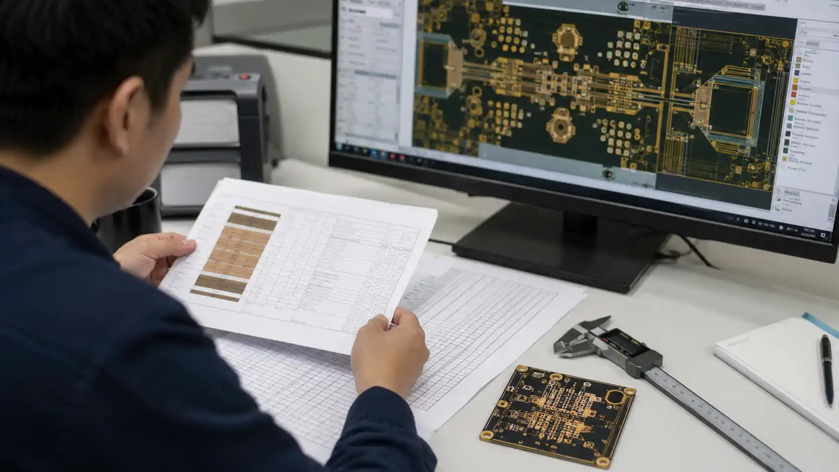
A good prototype order should give the PCB manufacturer enough information to understand the RF path, not just the copper pattern.
Quick Summary
- RF and microwave PCBprototype risk can be reduced by confirming material, stackup, impedance, copper thickness, connector launch, via structure, surface finish, and testing requirements before production.
- Gerber files alone are not enough for serious high-frequency PCB
- Buyers should clearly provide working frequency, material preference, controlled impedance requirements, board thickness, copper thickness, surface finish, RF connector details, and application background.
- The goal of prototype production is not only to receive samples. The goal is to build a sample that can be repeated in future batch production.
Start With Complete Files
Many prototype problems begin before quotation. The buyer sends Gerber files, but the stackup, material, impedance, and working frequency are missing. The factory quotes the board as a normal PCB with high-frequency material, and the risk is hidden until testing.
A complete prototype package should include:
- Gerber files
- Drill files
- PCB stackup
- Material preference
- Working frequency
- Controlled impedance table
- Board thickness
- Copper thickness
- Surface finish
- Connector type
- Quantity
- Application background
If the material is not yet fixed, working frequency and application background become even more important. The manufacturer can then review whether the proposed laminate and stackup — whether Rogers, PTFE, Taconic, F4B, or a hybrid stackup — are realistic for production.
Confirm the Material Before Layout Changes
Material choice should be reviewed and confirmed before the prototype is released for production. Some RF projects can use cost-balanced materials. Some microwave paths require low-loss laminates. Some antenna designs are sensitive to Dk value and board thickness. If the material is changed after layout, trace width, impedance, antenna tuning, and signal loss may all shift.
The material review should check:
- Dk and Df values
- Dielectric thickness
- Copper thickness
- Copper type
- Material availability
- Prototype lead time
- Batch availability
- Manufacturing difficulty
A prototype built with a temporary material may support early design checking, but it should not be treated as proof of final RF performance.
Lock the Stackup Early
Stackup is part of the RF design. It should not be decided casually during production.
A complete stackup review should define:
- Layer count
- Material type
- Dielectric thickness
- Copper thickness
- RF signal layer
- Ground reference plane
- Power layer (if used)
- Final board thickness
- Via structure
- Controlled impedance target and tolerance
If dielectric thickness changes, impedance changes. If copper thickness changes, trace geometry changes. If the ground reference changes, the RF return path may become unstable.
For prototypes, the stackup should be as close as possible to the intended production stackup. Otherwise, the prototype result may not accurately predict batch performance. See IPC-2141A for controlled impedance stackup guidelines.
Treat Controlled Impedance as a Manufacturing Requirement
Controlled impedance should be clearly stated before quotation.
A trace does not become controlled impedance simply because it looks like an RF line. The manufacturer needs the target impedance value, tolerance, layer location, trace structure, reference plane, and stackup confirmation.
Common mistakes include:
- No impedance table provided
- No tolerance requirement specified
- Stackup missing from the package
- Wrong copper thickness assumed
- Solder mask condition not confirmed
- No impedance coupon requirement stated
For RF and microwave boards, impedance review should happen before fabrication. Once the board is manufactured, impedance problems typically require a new production run. Impedance testing is defined under IPC TM-650.
Review Connectors Before Production
RF connector areas are one of the most common prototype failure points.
SMA, SMP, edge launch, U.FL, IPEX, board-to-board RF connectors, and coaxial interfaces all require careful transition design from the connector pad to the PCB trace.
Review these points before production:
- Connector footprint accuracy
- Pad-to-trace transition geometry
- Ground via placement
- Reference plane continuity
- Mounting holes
- Cable stress tolerance
- Surface finish compatibility
- Assembly method
A good RF material cannot compensate for a poor connector launch. If the prototype will be used for RF testing, the connector area deserves extra attention before production starts.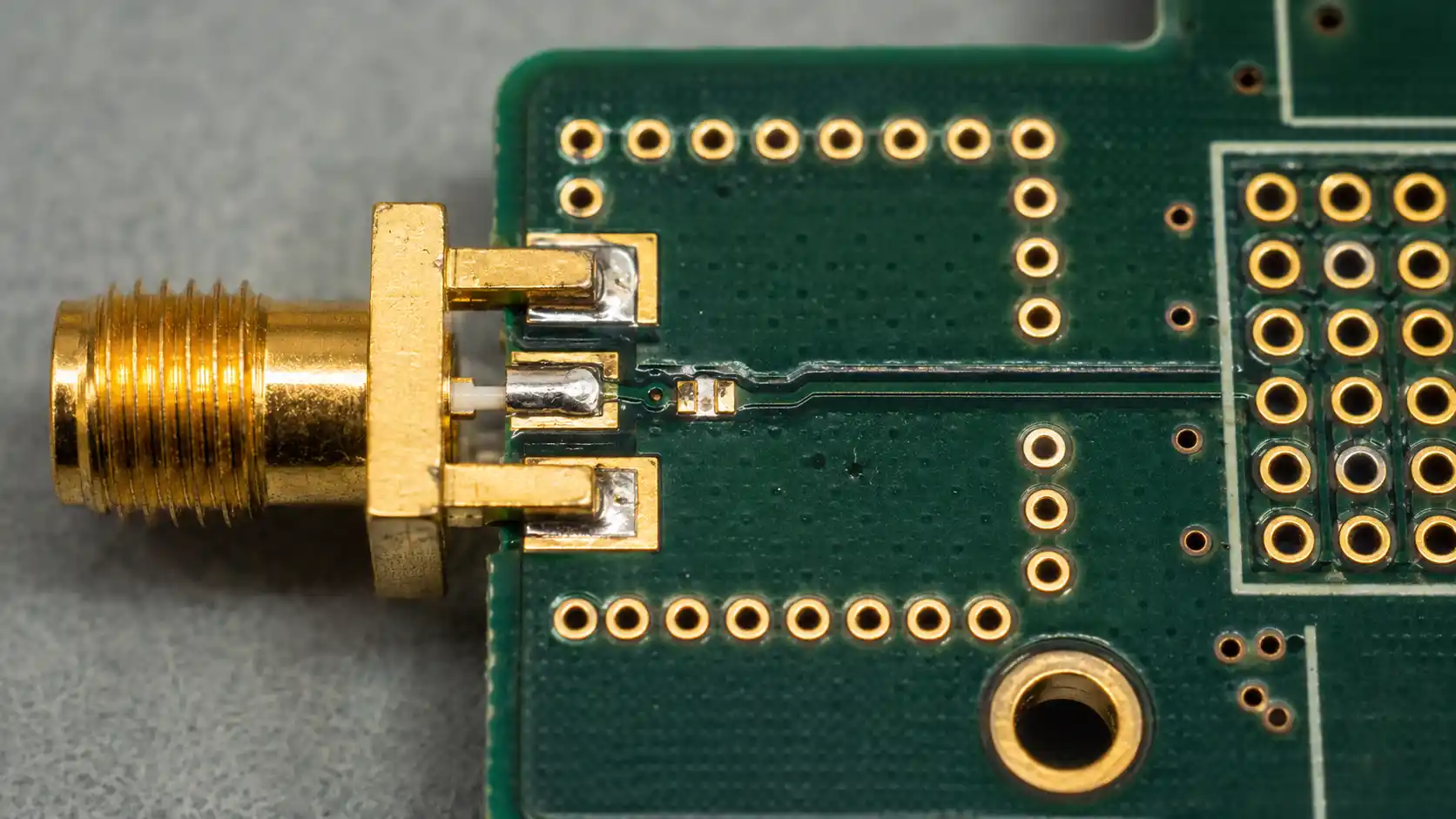
Check Vias, Grounding, and Return Path
Vias may appear to be small details, but they can significantly affect RF behavior.
A via may be used for signal transition, grounding, shielding, via fence, thermal transfer, or connector grounding. In microwave designs, via length and stub behavior can become visible during testing.
The review should include:
- Signal via size
- Ground via spacing
- Via stub length
- Via fence placement
- Anti-pad clearance
- Plated through-hole reliability
- Connector grounding vias
- Layer transition path
Ground reference continuity is equally important. If the RF trace crosses a split plane or loses its return path, the prototype may show reflection, radiation, or unstable test results.
Do Not Ignore Surface Finish
Surface finish is often selected by habit, but RF prototypes may need more careful consideration.
Common options include ENIG, immersion silver, OSP, lead-free HASL, hard gold for contact areas, or customer-specified finishes.
The choice should consider:
- Solderability requirements
- Connector areas
- RF-exposed pads
- Storage time
- Assembly process
- Contact wear
- Customer requirement
For early prototypes, it is generally better to use the finish intended for later production unless there is a clear technical reason to change it.
Plan for Prototype-to-Batch Transition
A prototype is only useful if it produces results that can be repeated in production.
Before placing the prototype order, buyers should ask:
- Will this material be available for batch production?
- Can the same stackup be consistently repeated?
- Will copper thickness remain the same?
- Will impedance testing be required in batch orders?
- Will the same connector type and surface finish be used?
- Will assembly conditions remain similar?
A prototype that passes RF testing with one material and one stackup may not represent the batch order if key parameters change later. This is especially important for radar systems, 5G equipment, and aerospace RF applications where performance repeatability is a hard requirement.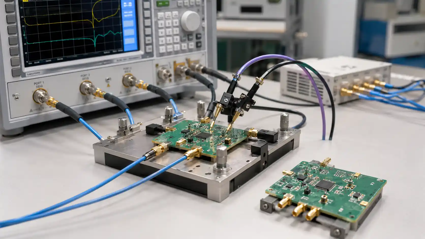
Common Prototype Mistakes
Common mistakes that lead to prototype failure or rework:
- Sending only Gerber files without supporting documentation
- No stackup information provided
- No working frequency specified
- No impedance table included
- Material selected based on price alone
- Changing material after layout is complete
- Ignoring connector launch design
- Using too few ground vias
- Ignoring via stubs at higher frequencies
- Selecting surface finish by purchasing habit
- Not discussing batch production requirements at prototype stage
Most of these issues can be avoided before fabrication if the manufacturer receives sufficient technical information at the quotation stage.
Conclusion
RF and microwave PCB prototype risk can be significantly reduced with better preparation. Material, stackup, controlled impedance, connector launch, vias, grounding, surface finish, and batch repeatability should all be reviewed before production starts.
For buyers, the best prototype is not simply the fastest sample. It is the sample that delivers reliable RF feedback and can guide the next production step with confidence.
A complete quotation package and early engineering review can prevent many avoidable prototype failures, reduce redesign cost, and improve confidence before batch manufacturing begins.
For technical reference, see IPC-2141A (Controlled Impedance Circuit Boards), IPC TM-650 (Test Methods Manual), and the Rogers MWI-2021 Impedance Calculator for material and impedance guidance.