
Rogers RO6010 is a ceramic-filled PTFE material with Dk of 10.2 at 10 GHz — the highest dielectric constant in the standard Rogers portfolio. High Dk materials are used for a specific purpose: reducing the physical size of resonant circuit elements. A patch antenna element resonant at 5 GHz on Rogers RO4350B (Dk 3.48) occupies approximately 16mm × 16mm. The same antenna on Rogers RO6010 (Dk 10.2) occupies approximately 9mm × 9mm — a 67% reduction in element area.
As a direct Rogers PCB factory with RO6010 in production inventory and plasma activation in-house, we build high Dk PCB for compact antenna arrays, bandpass filters, and miniaturized RF modules. This guide covers when RO6010 is the right material and how to specify it correctly.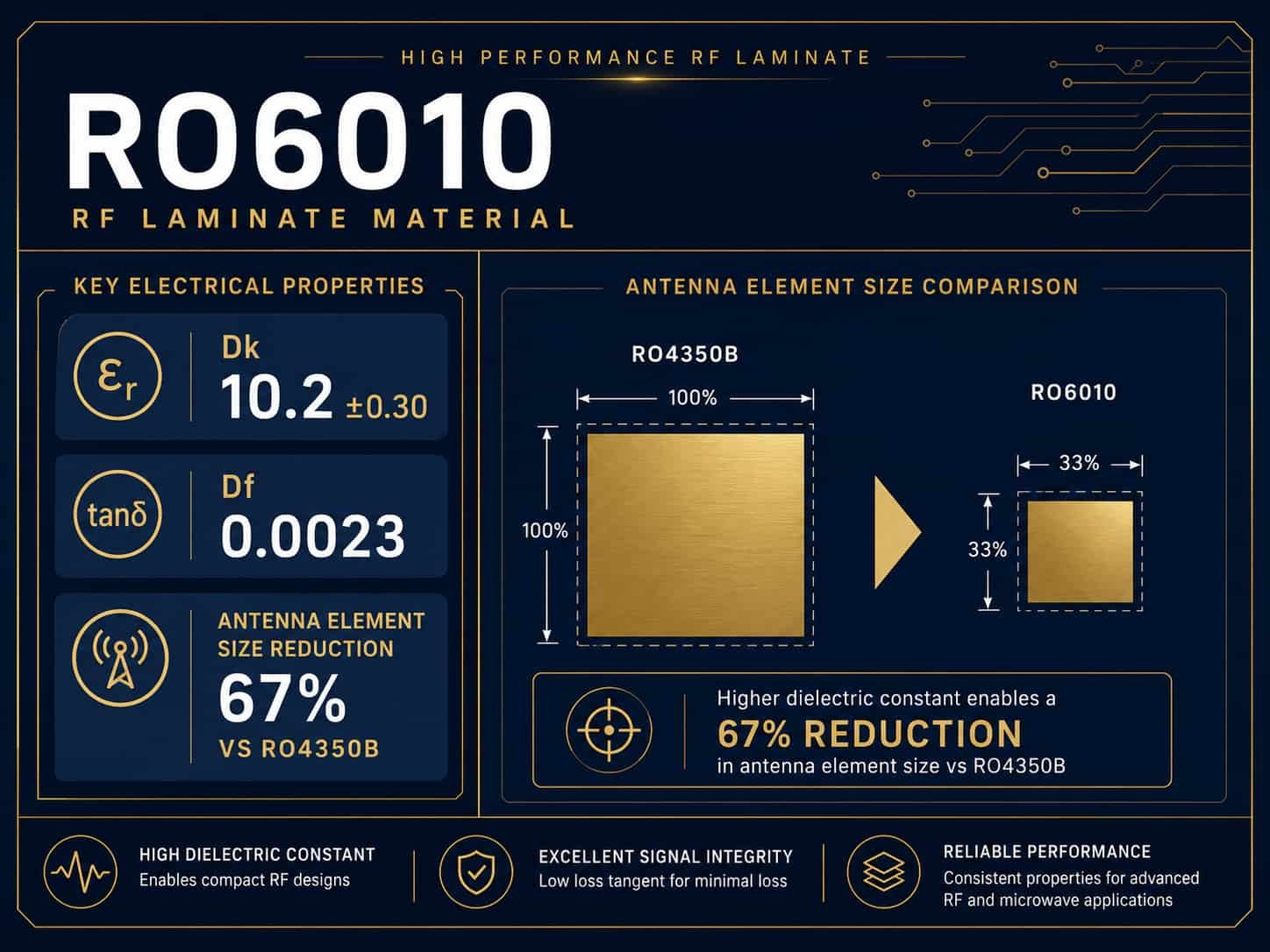
Quick Summary
Key point: Rogers RO6010 (Dk 10.2 ±0.30, Df 0.0023) is a ceramic PTFE material used when physical size reduction of resonant elements is the primary design driver. High Dk reduces antenna element dimensions proportional to 1/√Dk — RO6010 reduces element size by approximately 47% compared to RO4350B. The trade-off: higher Df than RO3003 (0.0010) or RO4350B (0.0037) — RO6010 Df of 0.0023 is adequate for filters and antennas where the Q factor is primarily set by conductor loss, not dielectric loss. RO6010 is a PTFE material requiring plasma activation.
Why High Dk PCB Is Used: The Miniaturization Principle
The physical size of resonant RF structures — patch antennas, resonator-based filters, coupled-line structures — scales inversely with the square root of the effective dielectric constant. Doubling the Dk reduces the resonant element dimensions by approximately 29%. Tripling the Dk reduces dimensions by approximately 42%.
- Element size ∝ 1/√(Dk_eff)
- At 10 GHz, patch antenna on RO4350B (Dk 3.48): approximately 8.0mm × 8.0mm
- At 10 GHz, patch antenna on RO3006 (Dk 6.15): approximately 6.0mm × 6.0mm — 25% size reduction
- At 10 GHz, patch antenna on RO6010 (Dk 10.2): approximately 4.7mm × 4.7mm — 41% size reduction vs RO4350B
- At 5 GHz, patch antenna on RO4350B: approximately 16mm × 16mm
- At 5 GHz, patch antenna on RO6010: approximately 9mm × 9mm
When to use high Dk: High Dk PCB materials are the correct choice when the physical aperture of the antenna or filter is constrained by system packaging — not when the designer simply wants smaller elements. Smaller elements on high Dk have narrower bandwidth and lower efficiency than larger elements on lower Dk. Use high Dk when you must fit within a space constraint, not as a default design choice.
Rogers RO6010 Material Properties
- Dk at 10 GHz: 10.2 ±0.30 — highest Dk in standard Rogers portfolio
- Df at 10 GHz: 0.0023 — acceptable for most compact antenna and filter applications
- Dk tolerance: ±0.30 — wider than lower-Dk Rogers materials (RO3003 ±0.04, RO4350B ±0.05)
- Dk temperature coefficient: approximately −425 ppm/°C — Dk decreases with temperature
- Material type: ceramic-filled PTFE — requires plasma activation, same as RO3003 and RT5880
- Maximum lamination cycles: 2 — same PTFE limit
- Bonding film: Rogers 2929 bondply for hybrid stackups
- Tg: greater than 500°C — PTFE, no practical glass transition
- Moisture absorption: 0.04% — low, good Dk stability in humid environments
Dk Tolerance — Important Design Consideration
Rogers RO6010’s Dk tolerance of ±0.30 is significantly wider than lower-Dk Rogers materials. This means the actual production Dk may be anywhere from 9.9 to 10.5. For resonant structures, this Dk variation produces a resonant frequency variation of approximately ±1.5% — at 10 GHz, the antenna resonance may shift by ±150 MHz between production lots. Designs using RO6010 must have adequate bandwidth to accommodate this variation, or the design must be tuned for each lot.
Design guidance: For narrowband filters using RO6010, plan for post-fabrication tuning or design the filter bandwidth wider than the minimum required to accommodate the Dk tolerance. For wideband patch antennas (bandwidth >5%), the Dk tolerance is typically within the antenna’s operating bandwidth and no special action is needed.
Rogers RO6010 vs RO3006 vs RO3010
Three Rogers materials cover the high Dk range. Understanding the differences helps select the correct material for each application.
Rogers RO3006 (Dk 6.15, Df 0.0020)
- Dk: 6.15 ±0.15 — moderate high Dk, tighter tolerance than RO6010
- Df: 0.0020 — lower Df than RO6010 (0.0023) — better for loss-sensitive applications
- Element size reduction: approximately 25% smaller than RO4350B at same frequency
- Best for: applications requiring moderate miniaturization with lower Df than RO6010
- Thicknesses: 0.127 / 0.254 / 0.635 / 1.270 mm
Rogers RO6010 (Dk 10.2, Df 0.0023)
- Dk: 10.2 ±0.30 — highest standard Rogers Dk, wider tolerance
- Df: 0.0023 — slightly higher than RO3006
- Element size reduction: approximately 41% smaller than RO4350B
- Best for: maximum miniaturization where physical space is tightly constrained
- Thicknesses: 0.127 / 0.254 / 0.635 / 1.27 / 1.905 / 2.54 mm
Rogers RO3010 (Dk 10.2, Df 0.0022)
- Dk: 10.2 ±0.30 — same Dk as RO6010
- Df: 0.0022 — very slightly lower than RO6010 (0.0023) — essentially equivalent
- The difference between RO6010 and RO3010 in practice: mostly availability and thickness range
- Thicknesses: 0.127 / 0.254 / 0.635 / 1.270 mm — fewer options than RO6010
- Best for: same applications as RO6010 — select based on required thickness
Rogers RO6010 Applications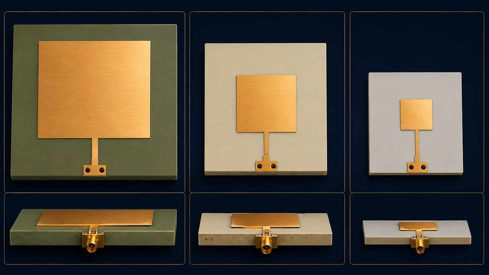
Compact Patch Antenna Arrays
The most common RO6010 application is compact patch antenna design where aperture area is constrained by system packaging. High Dk reduces each antenna element’s footprint, allowing more elements in the same aperture — increasing array gain without increasing physical size.
- Phased array with fixed aperture: more elements on RO6010 = higher gain, narrower beam
- Handheld or body-worn devices: antenna must fit in a small physical form factor
- Conformal antenna arrays: tight radius requires small element pitch
- Dual-polarized arrays: high Dk allows tighter element spacing for cross-polarization isolation
- Frequency range: most common at S-band (2–4 GHz) and C-band (4–8 GHz) where RO4350B elements would be too large for the application
Bandpass Filters
Microwave bandpass filters based on coupled half-wavelength resonators benefit from high Dk in the same way as patch antennas — each resonator section is shorter on high Dk material, allowing more resonator stages in the same physical length.
- Coupled-line bandpass filter: resonator length proportional to 1/√Dk — RO6010 reduces length by 41% vs RO4350B
- Edge-coupled filters: compact high-order filters for applications with strict form factor limits
- Diplexers and multiplexers: multiple filter sections in constrained space
- Frequency range: S-band through Ku-band — wherever physical size is the binding constraint
- Trade-off: filter Q factor is lower on high Dk due to slightly higher Df — acceptable for most applications
Miniaturized Impedance Matching Networks
Quarter-wave and half-wave transmission line sections used for impedance matching are shorter on high Dk material — useful when the matching network must fit between closely spaced components.
- Quarter-wave transformer on RO6010 at 10 GHz: approximately 4.7mm vs 8.0mm on RO4350B
- Used in: power amplifier output matching, LNA input matching, antenna feed transitions
Dielectric Resonator Oscillator (DRO) Substrate
High Dk PCB is sometimes used as the substrate in dielectric resonator oscillator circuits where the high Dk of the substrate helps reduce the overall circuit size.
Manufacturing Process for Rogers RO6010
Rogers RO6010 is a PTFE ceramic material. Its manufacturing process is identical to Rogers RO3003 and RT5880 in all critical areas — plasma activation, PTFE-specific drilling, Rogers 2929 bondply, and 2-cycle lamination limit.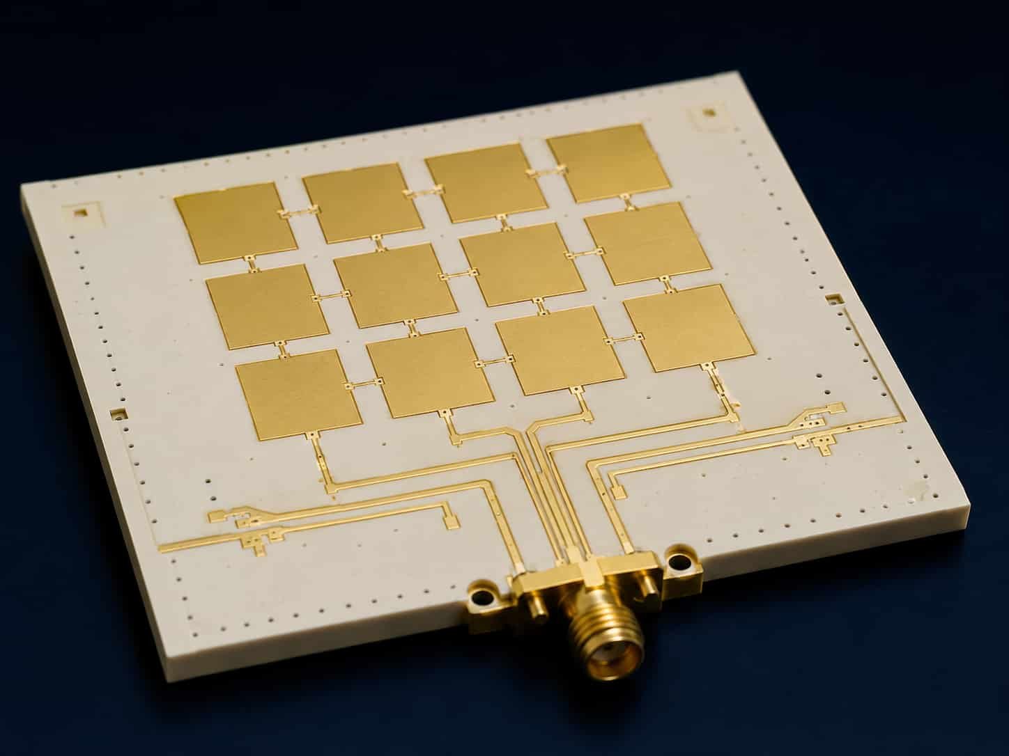
Hole Wall Activation
- Plasma activation: mandatory — same as RO3003 and RT5880
- Without activation: copper will not bond to RO6010 PTFE ceramic hole walls
- Ceramic filler: the ceramic particles in RO6010 make the PTFE surface slightly different from pure PTFE — plasma parameters are confirmed for RO6010 specifically
Drilling
- PTFE-specific parameters: same spindle speed and feed rate requirements as RO3003
- Ceramic content: the ceramic filler in RO6010 is harder than pure PTFE — slightly different drill parameters than RT5880 (PTFE glass) confirmed at our factory
- Hole wall quality: inspect after drilling — ceramic particles can cause local irregularities if parameters are not optimized
Bonding Film
- Rogers 2929 bondply: required for RO6010 hybrid stackups
- Same as RO3003 and RT5880 — NOT RO4450F
- Maximum lamination cycles: 2
Controlled Impedance on RO6010
RO6010’s Dk of 10.2 produces narrow traces for 50Ω microstrip — narrower than on lower-Dk materials for the same substrate thickness.
- 50Ω microstrip on RO6010 0.254mm, 1 oz copper: trace width ≈ 0.22mm (8.7 mil)
- 50Ω microstrip on RO6010 0.635mm, 1 oz copper: trace width ≈ 0.55mm (22 mil)
- 50Ω microstrip on RO6010 1.27mm, 1 oz copper: trace width ≈ 1.10mm (43 mil)
- Dk tolerance ±0.30: produces approximately ±1.5% impedance variation between lots — within ±10% standard tolerance
- TDR verification: every production lot — confirmed using production Dk from Rogers material certificate
Rogers RO6010 Available Thicknesses
- 127 mm: very compact designs at higher frequencies
- 254 mm: standard for most compact antenna applications at X-band and above
- 635 mm: S-band and C-band compact antennas
- 270 mm: lower frequency or thicker substrate requirements
- 905 mm: mechanical substrate applications
- 540 mm: thick substrate for specific filter or resonator designs
Rogers RO6010 Production at Riching PCB
- RO6010 thicknesses in inventory: 0.127 / 0.254 / 0.635 / 1.27 / 1.905 / 2.54 mm
- Plasma activation: in-house — confirmed for RO6010 ceramic PTFE
- Rogers 2929 bondply: in stock for hybrid stackups
- Controlled impedance: ±10% standard, ±8% advanced — TDR verified every lot
- Minimum line width: 2.5 mil advanced — needed for narrow traces on high Dk substrate
- Maximum lamination cycles: 2 — strictly observed
- IPC Class 3: available on request
What to Specify for Rogers RO6010 PCB Quotation
- Rogers RO6010 — confirm substrate thickness from standard range
- Copper weight per layer — affects trace width on high Dk substrate
- Complete stackup with layer sequence, copper weight, dielectric thickness
- Controlled impedance — target, tolerance, layer, structure
- Operating frequency — helps DFM confirm trace width feasibility
- Application type — compact antenna or filter
- Bandwidth requirement — narrow band designs need Dk tolerance consideration
- IPC Class and quantity
For the complete file checklist, see What Files Are Needed for a High Frequency PCB Quotation?. For Rogers high Dk material comparison, see Rogers PCB Material Selection Guide.
Conclusion
Rogers RO6010 (Dk 10.2, Df 0.0023) is the material of choice when physical miniaturization of resonant RF elements is the binding design constraint — compact patch antenna arrays, bandpass filters, and matching networks where aperture area or PCB real estate is tightly limited. The 41% element size reduction compared to RO4350B comes at the cost of wider Dk tolerance (±0.30), slightly higher Df, and PTFE manufacturing requirements. For designs where these trade-offs are acceptable, RO6010 provides the most compact resonant structures available in standard Rogers PCB materials.
As a direct Rogers PCB factory with RO6010 in production inventory, plasma activation in-house, and Rogers 2929 bondply in stock, we build RO6010 PCB for compact antenna and filter applications. Submit your design for DFM review — we confirm trace width feasibility at the specified frequency and Dk tolerance impact on your antenna bandwidth before production begins.