
RF and mmWave Test Fixture PCB Design — Probe Pad Geometry and De-Embedding Structures
A test fixture PCB exists purely to characterize a device or material under controlled, known conditions — its own electrical properties must be understood precisely enough to be mathematically removed (de-embedded) from the measurement, leaving only the device under test's actual performance. This makes fixture design a different discipline from product RF PCB design: the fixture's own trace, via, and connector properties matter as much as, or more than, they would in a production board, because every uncharacterized parasitic becomes measurement error. This guide covers probe pad geometry, calibration standard design, and the manufacturing tolerances that determine fixture accuracy.
Home » RF and mmWave Test Fixture PCB Design — Probe Pad Geometry and De-Embedding Structures
Table of Contents
Probe Types and Pad Geometry
| Probe Type | Typical Frequency | Pad Pitch | Pad Geometry Requirement |
|---|---|---|---|
| GSG (Ground-Signal-Ground) probe | DC–110GHz depending on model | 100–250µm common | Coplanar pads, tight pitch tolerance, flat clean surface |
| GS (Ground-Signal) probe | Lower frequency, simpler fixtures | 150–250µm common | Fewer constraints than GSG, still needs flat surface |
| Coaxial probe (cable-based) | Broadband, lower frequency emphasis | N/A — connector-based | Standard connector footprint |
GSG (Ground-Signal-Ground) microprobes are the standard approach for on-wafer and fixture-level characterization from a few GHz through mmWave frequencies, offering a well-defined, repeatable contact geometry that connector-based test setups cannot match at the highest frequencies. Pad pitch must match the specific probe model exactly — a mismatch of even a small fraction of the specified pitch degrades contact quality and measurement repeatability, independent of how well the rest of the fixture is designed.
Calibration Standards on the Fixture
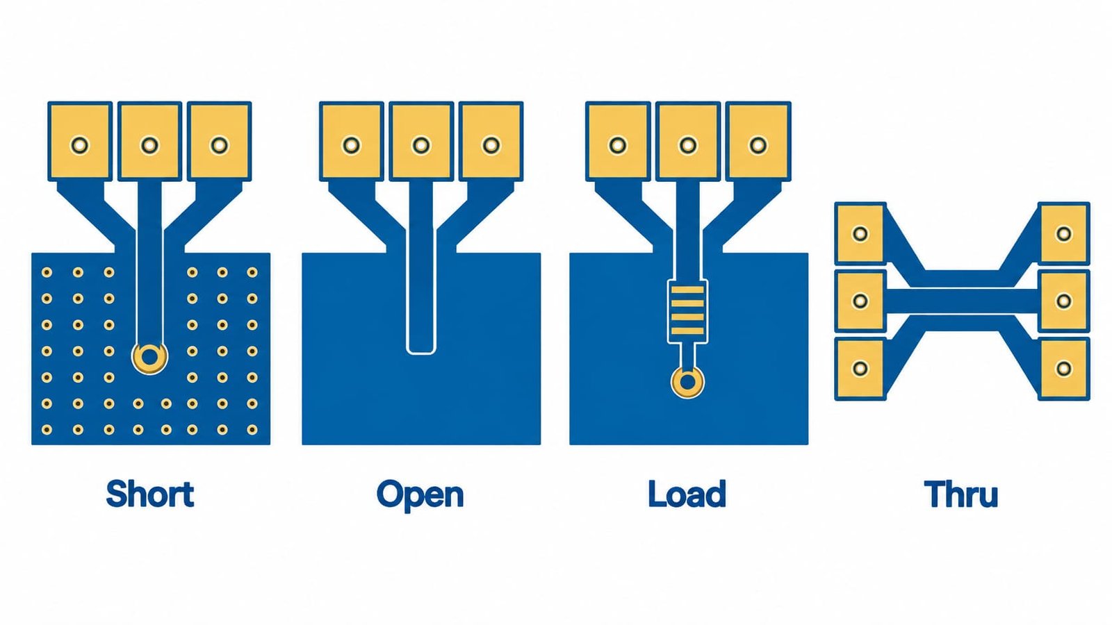
| Calibration Standard | Purpose | PCB Fixture Requirement |
|---|---|---|
| Short | Reference for calibration algorithm | Precisely known short-circuit structure at the reference plane |
| Open | Reference for calibration algorithm | Precisely known open-circuit structure, often a small stub |
| Load (typically 50Ω) | Reference for calibration algorithm | Matched termination structure, accuracy affects cal quality |
| Thru | Establishes reference plane, enables de-embedding | Known-length line connecting two ports |
| Line/Reflect/Line (TRL) | Alternative method, preferred at mmWave | Multiple known-length line structures |
Short-Open-Load-Thru (SOLT) and Thru-Reflect-Line (TRL) are the two most common calibration methodologies implemented directly on a test fixture PCB. TRL is generally preferred at mmWave frequencies because it relies on known transmission line lengths rather than lumped-element standards, which become difficult to characterize precisely as frequency increases. Whichever method is used, the calibration standards must be fabricated with the same process and material as the actual device-under-test paths on the fixture — any difference between the cal standard fabrication and the DUT path fabrication introduces error that calibration cannot remove.
De-Embedding Structure Design
De-embedding relies on precisely knowing the electrical length and loss of the fixture structure between the calibration reference plane and the device under test. This is why simulation-ready material data matters more for fixture design than almost any other RF PCB application — the fixture’s own Dk, Df, and physical dimensions must be known accurately, not assumed from nominal datasheet values, because any error here becomes a direct error in the characterization result for whatever device the fixture is measuring.
Manufacturing Tolerance for Fixture Accuracy
| Parameter | Standard Tolerance | Impact on Fixture Accuracy |
|---|---|---|
| Probe pad pitch and position | ±0.005–0.01mm for GSG at mmWave | Directly affects probe contact quality and repeatability |
| Trace length matching (cal standards vs DUT paths) | As tight as practical, confirm with fabricator | Length mismatch introduces phase error calibration can't remove |
| Substrate Dk/Df measured value | Request actual lot data, not nominal | De-embedding accuracy depends on knowing actual line properties |
| Surface finish flatness at probe pads | ENIG preferred for flat, repeatable contact | Uneven surface causes inconsistent contact resistance |
A test fixture’s accuracy is only as good as the least-controlled dimension on the board. Unlike a production RF board where a small trace width deviation might be absorbed within an overall performance margin, a fixture’s job is precision characterization — request tighter-than-standard tolerance confirmation from your fabricator specifically for probe pad geometry and cal standard structures, even if the rest of the board uses standard tolerance.
DFM Checklist for RF/mmWave Test Fixture PCB
- Confirm probe pad pitch and geometry against the specific probe model’s datasheet, not a generic GSG pattern
- Request material lot Dk/Df certificate specifically for the fixture panel, since de-embedding accuracy depends on knowing actual fixture line properties
- Specify ENIG surface finish for probe contact areas — flat, repeatable surface is more important here than for a production board’s general solderability needs
- Confirm fabrication process consistency between calibration standard structures and DUT test paths — both should come from the same panel and lot
- For TRL calibration, confirm your fabricator can hold the trace length tolerance the calibration method requires across multiple line structures
RF and mmWave Test Fixture PCB — Q&A
Common questions about probe pad geometry, calibration methods, and material data requirements for test fixture PCB design.
What is a GSG probe pad and why does its geometry matter?
A coplanar contact structure used with microprobes for RF characterization from a few GHz through mmWave. Pad pitch must match the specific probe model exactly — even a small mismatch degrades contact quality and repeatability.
What is the difference between SOLT and TRL calibration for test fixtures?
SOLT uses lumped-element standards, while TRL relies on known transmission line lengths. TRL is generally preferred at mmWave because lumped elements become difficult to characterize precisely as frequency increases.
Why does a test fixture need more precise material data than a typical RF PCB?
De-embedding relies on precisely knowing the fixture's electrical length and loss. Any error in actual Dk, Df, or dimensions becomes a direct error in the characterization result for the device being measured.
Test Fixture PCB — Probe Pad Precision and Material Lot Data
GSG pad geometry matched to your specific probe model, ENIG finish for repeatable contact, material lot Dk/Df certificates for de-embedding accuracy. Process consistency verified between cal standards and DUT paths.
Simulation-Ready Material Data → WhatsAppRequest a PCB Quote
Upload your Gerber ZIP file and project requirements. Our engineering team will review your PCB material, stackup, impedance needs, surface finish, and production quantity before quoting.
Please prepare:
- Gerber files in ZIP format
- PCB material or stackup requirements
- Controlled impedance notes if available
- Prototype or batch production quantity