
How to Choose PCB Materials for Antenna Applications
Antenna PCB material selection is one of the most important decisions in RF and high frequency circuit design. Unlike general electronic boards, antenna PCBs are closely related to signal radiation, impedance matching, dielectric stability, and final wireless performance.
For antenna applications, the PCB is not only a mechanical carrier. It can directly affect antenna efficiency, signal loss, frequency response, and product consistency.
This is why antenna PCB projects often require high frequency materials such as Rogers, PTFE, Taconic, F4B, or FR4 plus high frequency hybrid stackups.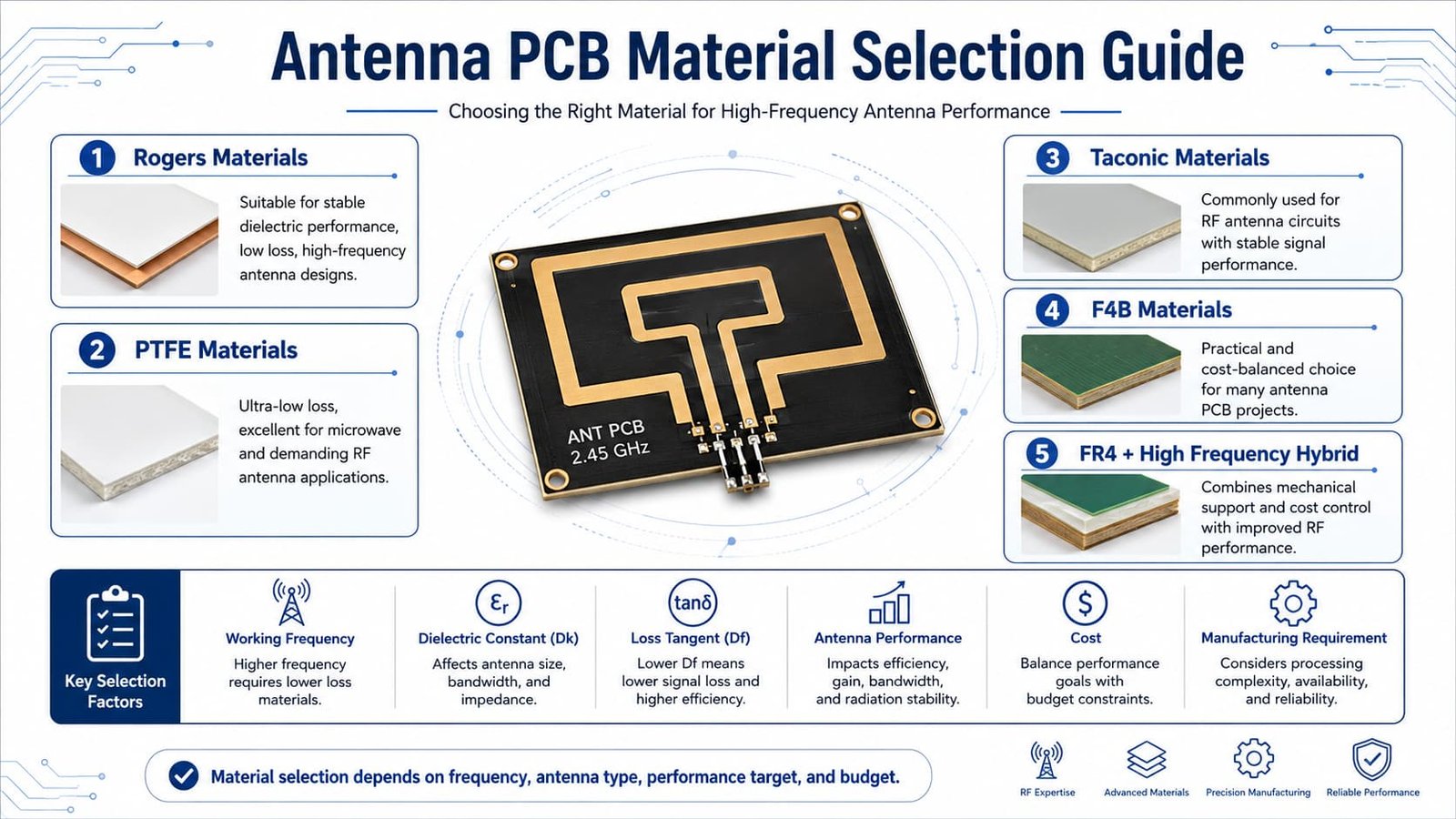
Why Material Selection Matters for Antenna PCB
Antenna PCB performance is strongly affected by the material underneath the copper pattern.
In many antenna designs, the copper trace, dielectric layer, board thickness, ground plane, and surrounding mechanical structure work together. If the material is not suitable, the antenna may show poor impedance matching, higher signal loss, frequency shift, lower radiation efficiency, or unstable production repeatability.
For this reason, antenna PCB material selection should be reviewed before fabrication, especially when the project involves RF modules, 5G devices, satellite communication, radar electronics, wireless infrastructure, or precision test equipment.
Key Factors When Choosing Antenna PCB Materials
1. Operating Frequency
The first question is always the operating frequency.
A lower-frequency wireless product may be able to use standard FR4 in some cases. However, as frequency increases, signal loss and material stability become more important. For RF, microwave, radar, satellite, and 5G antenna applications, high frequency PCB materials are often preferred.
Typical antenna PCB applications may include:
WiFi antenna modules
Bluetooth antenna boards
GPS antenna systems
RF communication modules
5G antenna devices
Radar antenna PCBs
Satellite communication antennas
Industrial wireless equipment
IoT antenna boards
If the antenna operates at a higher frequency or requires stable RF performance, material choice becomes more critical.
2. Dielectric Constant
Dielectric constant, also known as Dk, affects signal speed, wavelength, antenna size, and impedance.
For antenna PCB design, Dk is not just a material number. It can influence antenna geometry and frequency behavior. A higher Dk material may allow a smaller antenna size, while a lower Dk material may help reduce certain types of loss and support wider bandwidth depending on the design.
However, the most important point is stability. A stable Dk helps maintain predictable antenna performance from prototype to batch production.
3. Dissipation Factor
Dissipation factor, also known as Df, affects signal loss.
For antenna PCBs, lower Df materials are often preferred when signal efficiency and transmission stability are important. This is especially relevant for microwave antennas, radar antennas, satellite communication antennas, and high frequency RF modules.
If the Df is too high for the application, the circuit may experience higher signal loss and reduced RF efficiency.
This is why many antenna PCB projects use low-loss materials instead of ordinary FR4.
4. Board Thickness
Board thickness can directly affect antenna impedance, bandwidth, mechanical structure, and final RF performance.
For some antenna designs, the thickness of the dielectric layer is part of the RF structure. Changing board thickness without engineering review may shift the antenna frequency or affect impedance matching.
Before production, the antenna PCB stackup should confirm:
Final board thickness
Dielectric thickness
Copper thickness
Layer count
Material type
Ground plane structure
Impedance target
Surface finish
If the design requires controlled impedance, the board thickness and dielectric thickness must be reviewed together.
5. Copper Accuracy and Pattern Control
Antenna PCBs are sensitive to copper geometry.
The antenna trace width, feed line width, clearance, copper shape, ground connection, and via placement may all influence performance. If the finished copper pattern deviates from the design, antenna behavior may change.
Important manufacturing controls include:
Trace width tolerance
Etching accuracy
Copper thickness control
Ground copper accuracy
Via position control
Surface finish consistency
Final inspection
For small antenna structures or high frequency antenna modules, tight copper control is especially important.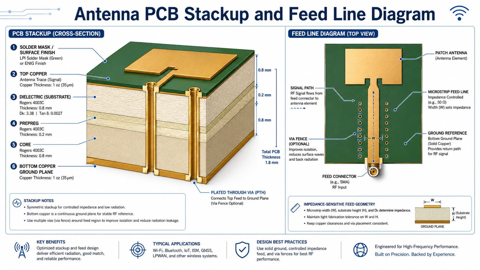
6. Controlled Impedance
Controlled impedance is critical for many antenna PCB designs.
The antenna feed line usually needs to match the system impedance, often 50 ohms in many RF applications. If impedance is not controlled properly, signal reflection may increase and antenna efficiency may decrease.
Controlled impedance depends on:
Material Dk
Dielectric thickness
Trace width
Copper thickness
Reference ground plane
Solder mask
Manufacturing tolerance
Common PCB Materials for Antenna Applications
Rogers Materials
Rogers materials are widely used in antenna, RF, microwave, and communication PCB applications.
Rogers has several material families used in antenna-related projects, including RO3000, RO4000, RT/duroid, RO4500, and RO4700 series. Rogers describes RO4500 as materials engineered for antenna market requirements, and RO4700 as antenna grade laminates. These are useful external references when explaining antenna material selection.
Rogers antenna PCB materials may be suitable for:
RF antenna boards
5G antenna modules
Wireless infrastructure
Microwave antenna circuits
Radar antenna PCBs
Satellite communication antenna boards
PTFE Materials
PTFE materials are often selected for low-loss RF and microwave antenna applications.
For antenna systems where signal loss is critical, PTFE-based laminates can provide stable high frequency performance. They are commonly considered for radar, satellite communication, microwave antenna, aerospace, and precision RF applications.
However, PTFE PCB manufacturing is more difficult than standard FR4 processing. Drilling, plating, lamination, copper bonding, and dimensional stability require experienced process control.
Taconic Materials
Taconic materials are also used in RF and microwave PCB projects, including antenna applications.
They may be suitable when the design requires stable dielectric performance, low loss, and high frequency material support. The right Taconic material should be selected based on working frequency, antenna structure, Dk, Df, board thickness, and production feasibility.
F4B Materials
F4B materials can be considered for antenna PCB projects where performance, material availability, and cost control need to be balanced.
For some RF antenna boards, wireless communication boards, and industrial RF devices, F4B can be a practical option. However, it should still be reviewed according to frequency, loss requirement, impedance, and stackup design.
FR4 Plus High Frequency Hybrid Stackups
Not every antenna PCB project needs to use high frequency material for the entire board.
In some multilayer designs, engineers may use high frequency material only on the RF antenna layer, while using FR4 for supporting layers. This structure can help balance RF performance, mechanical strength, and production cost.
However, hybrid stackups require careful review because different materials may have different thermal expansion, bonding behavior, and lamination requirements.
Antenna PCB Material Selection by Application
Wireless Communication Devices
For wireless devices such as WiFi, Bluetooth, GPS, and IoT products, material choice depends on operating frequency, product size, antenna structure, and cost target.
Some simple low-frequency antenna designs may use FR4, but higher-performance RF antenna boards may require more stable high frequency materials.
5G Antenna Modules
5G antenna modules often require stable signal transmission, tight dimensional control, and low-loss material selection.
For these applications, Rogers, PTFE, or other high frequency materials may be considered based on the working frequency and final product requirement.
Radar Antenna PCB
Radar antenna PCB projects often require microwave PCB materials with low signal loss and stable electrical performance.
For radar antenna boards, material selection, copper accuracy, controlled impedance, plated through-hole reliability, and surface finish should all be reviewed before production.
Satellite Communication Antennas
Satellite communication antenna PCBs require stable high frequency performance and reliable manufacturing quality.
These projects often use low-loss materials and controlled impedance structures. PTFE, Rogers, and other advanced materials may be reviewed depending on frequency, environment, and signal requirement.
Antenna Modules
Antenna module PCB projects may combine antenna traces, RF feed lines, matching circuits, connectors, grounding structures, and multilayer stackups.
For these projects, the PCB manufacturer should review the material, stackup, impedance, copper thickness, via structure, and surface finish before production.
External Design Reference for RF Layout
For antenna PCB projects, material selection is only one part of the design. RF layout, feed line design, grounding, decoupling, via placement, and antenna tuning can also affect performance.
A useful technical reference is Infineon’s antenna design and RF layout application note, which covers RF trace, PCB stackup, antenna grounding, and layout considerations.
Manufacturing Requirements for Antenna PCB
Antenna PCB manufacturing requires more than simply producing copper patterns.
The manufacturer should control:
Material verification
Stackup accuracy
Dielectric thickness
Trace width and spacing
Copper thickness
Controlled impedance
Drilling accuracy
Plated through-hole quality
Surface finish
Final inspection
For RF antenna and microwave antenna projects, engineering review before production is important because small changes in material or geometry may affect final performance.
What Information Is Needed for Antenna PCB Quotation?
To quote an antenna PCB project accurately, the manufacturer usually needs:
Gerber files
Drill files
PCB stackup
Material requirement
Operating frequency
Board thickness
Copper thickness
Surface finish
Controlled impedance requirement
Quantity
Antenna type or application
Prototype or batch production requirement
Special tolerance requirements
If the material is not fixed, the manufacturer can review possible options such as Rogers, PTFE, Taconic, F4B, or hybrid stackups according to your antenna design.
How to Reduce Antenna PCB Material Risk
Before production, engineers and buyers should confirm:
The operating frequency is clear
The material Dk and Df are suitable
The board thickness is confirmed
The feed line impedance is defined
The ground plane structure is reviewed
The copper tolerance is manufacturable
The surface finish is suitable for assembly
The manufacturer has RF PCB experience
For antenna PCB projects, material substitution should not be made casually. Even if two materials seem similar, their Dk, Df, thickness tolerance, copper type, and processing behavior may be different.
Conclusion
Choosing PCB materials for antenna applications requires a balance between electrical performance, antenna structure, manufacturing feasibility, cost control, and final product reliability.
For simple wireless devices, standard materials may be enough in some cases. For RF antenna boards, microwave antennas, radar antenna PCBs, satellite communication antennas, 5G antenna modules, and wireless infrastructure, high frequency materials such as Rogers, PTFE, Taconic, F4B, or hybrid stackups are often reviewed.
The best material depends on operating frequency, Dk, Df, board thickness, impedance requirement, copper accuracy, stackup structure, and production capability.
For antenna PCB projects, early engineering review can help reduce material risk and improve production consistency.