
Dk and Df in PCB: What They Mean, Why They Matter Above 5GHz, and How to Choose
Dk and Df are the two numbers that determine whether your high frequency PCB works or fails. Dk (dielectric constant) determines trace width, signal wavelength and antenna dimensions. Df (dissipation factor) determines how much signal energy you lose to heat per centimeter of trace. Below 5GHz, both numbers are small enough that FR4 often works. Above 5GHz, Df becomes the dominant constraint — and above 20GHz, both Dk and Df determine whether your design is even physically possible on a given material. This guide explains each parameter with real numbers, shows where each becomes critical, and maps frequency ranges to the correct material choice.
Table of Contents
Key point: Dk (dielectric constant) determines trace width for a given impedance — a 1% Dk variation shifts 50Ω microstrip trace width by approximately 0.5%. Df (dissipation factor) determines insertion loss — Rogers RO4350B (Df 0.0037) produces approximately 0.6 dB/cm at 10 GHz; standard FR4 (Df ~0.020) produces approximately 3 dB/cm at the same frequency. For RF PCB above 1 GHz, Df is the primary material selection criterion. Rogers RO4350B (Df 0.0037) is standard for 1–12 GHz. Rogers RO3003 (Df 0.0010, PTFE) is required for Ka-band and 77 GHz. Rogers RT5880 (Df 0.0009, PTFE) is standard for wideband EW 2–18 GHz. Riching PCB manufactures controlled impedance RF PCB with TDR verification on every lot. No MOQ, 5–7 day prototype.
Dk — What It Is and Why It Matters
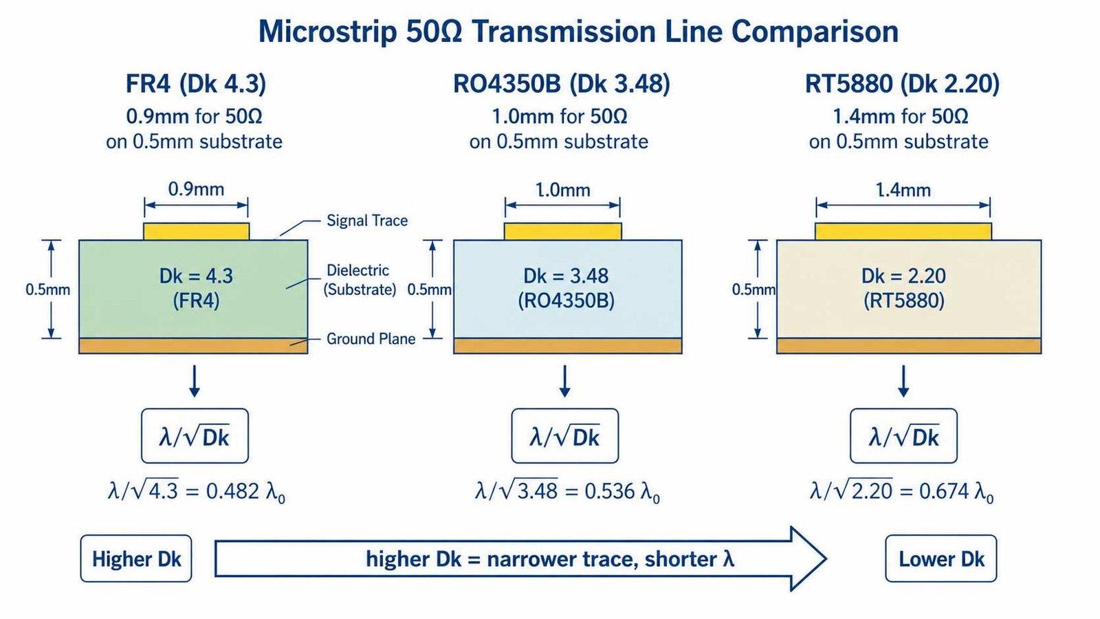
Dk (dielectric constant, also called relative permittivity) measures how much a material slows down electromagnetic waves and stores electric field energy compared to free space. In practical PCB design, Dk has four direct effects:
- Trace width for a given impedance: higher Dk → narrower 50Ω trace. On 0.508mm substrate with 1oz copper, FR4 (Dk 4.3) requires ~0.9mm trace for 50Ω; RT5880 (Dk 2.20) requires ~1.42mm. This is why RT5880 is not used for 77GHz radar arrays — the trace is too wide to achieve λ/2 element spacing.
- Signal wavelength inside the material: λ_effective = λ_free / √Dk. Higher Dk → shorter electrical wavelength → quarter-wave stubs, filter resonators and antenna elements are physically smaller. This is a design advantage (miniaturization) or disadvantage (tighter geometry tolerance) depending on application.
- Phase velocity: signals travel at c/√Dk through the material. Higher Dk → slower phase velocity → useful for time-delay lines; undesirable for minimizing signal path length in phased arrays.
- Dk tolerance and uniformity: Dk variation across a panel affects impedance, antenna resonant frequency and phase match in array designs. Rogers RO3003 Dk tolerance is ±0.04 — a tighter specification than most hydrocarbon materials, which is why it is the standard for 77GHz radar arrays where element-to-element phase error must be minimized.
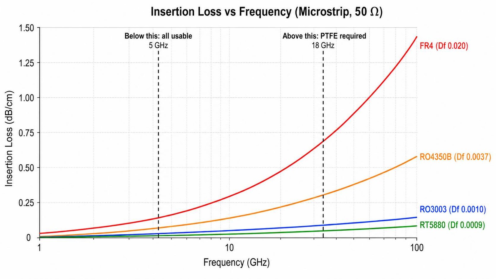
Df (dissipation factor, also called loss tangent) measures how much signal energy is absorbed by the dielectric material and converted to heat as the signal travels through it. Df has one primary practical effect: insertion loss per unit length.
Insertion loss due to dielectric: L_dielectric ≈ 27.3 × Df × f × √Dk (dB/m), where f is in GHz. This formula shows that insertion loss scales linearly with both Df and frequency. Double the frequency → double the dielectric loss. Double the Df → double the loss at every frequency. This is why materials that work at 5GHz fail at 28GHz — the Df term scales with frequency, making the loss penalty grow with every GHz.
Worked example: Df impact at 28GHz
A 10cm feed network at 28GHz:
- FR4 (Df 0.020): ~12 dB insertion loss — unusable
- RO4350B (Df 0.0037): ~4.5 dB — marginal for most designs
- RO3003 (Df 0.0010): ~1.2 dB — acceptable
- RT5880 (Df 0.0009): ~1.0 dB — best available in standard stock
The 3.3dB difference between RO4350B and RO3003 at 28GHz is not a minor performance factor — it is equivalent to the noise figure degradation of a poor LNA. For a Ka-band receiver where the system NF target is 3–4dB, losing 3.3dB in the feed network before the LNA is a design failure.
Material Comparison — Dk, Df and Insertion Loss
| Material | Dk | Df | Loss @10GHz (dB/cm) | Loss @28GHz (dB/cm) | Best For |
|---|---|---|---|---|---|
| FR4 standard | 4.3 | 0.020 | ~0.45 | ~1.2 | <1GHz only |
| Rogers RO4350B | 3.48 | 0.0037 | ~0.18 | ~0.45 | 1–18GHz |
| Rogers RO4003C | 3.38 | 0.0027 | ~0.13 | ~0.32 | 1–20GHz |
| Rogers RO3003 | 3.0 | 0.0010 | ~0.05 | ~0.12 | 10–80GHz |
| Rogers RT5880 | 2.20 | 0.0009 | ~0.045 | ~0.10 | 2–40GHz wideband |
| Taconic TLY-5 | 2.22 | 0.0009 | ~0.045 | ~0.10 | EW wideband |
Decision Guide: Which Parameter Dominates at Each Frequency
| Frequency | Dk Constraint | Df Constraint | Recommended Material |
|---|---|---|---|
| <1GHz | Minimal | Minimal | FR4 or Hi-Tg FR4 |
| 1–5GHz | Moderate | Low | RO4350B or Hi-Tg FR4 |
| 5–12GHz | Significant | Moderate | RO4350B / RO4003C |
| 12–20GHz | Critical | High | RO4003C → RO3003 |
| 20–40GHz | Critical | Dominant | RO3003 |
| 40–80GHz | Critical | Dominant — PTFE only | RO3003 0.127mm |
| 2–18GHz wideband | Moderate | Dominant | RT5880 / TLY-5 |
Dk and Df in Practice — Common Design Errors
Error 1: Using FR4 Dk value in impedance simulation instead of actual substrate Dk
FR4 Dk varies between 4.1 and 4.7 depending on glass weave, resin content and frequency. Using a nominal Dk 4.3 in simulation when the actual material is 4.6 produces a 50Ω trace that is actually ~48Ω — a 4% error that causes visible return loss at frequencies above 5GHz. Always use the actual material datasheet Dk at the design frequency for impedance calculation.
Error 2: Ignoring Dk variation with frequency
Dk is not constant with frequency. Rogers RO4350B Dk at 1GHz is approximately 3.66; at 10GHz it drops to 3.48. For designs where the electrical length matters (filter resonators, antenna patches), use the Dk value at the operating frequency, not the value at 1GHz reported in some datasheets.
Error 3: Selecting material by Dk alone without checking Df
A material with Dk 3.0 and Df 0.020 (hypothetical) would match the trace width of RO3003 but produce 20× the insertion loss. Dk and Df must both be checked. A low Dk material with high Df is worse than a higher Dk material with low Df for most RF signal layer applications above 5GHz.
How to Read a PCB Material Datasheet for Dk and Df
- Check the test frequency: Dk and Df are frequency-dependent. A datasheet reporting Dk at 1GHz is not the same as one reporting at 10GHz. For designs above 5GHz, look for Dk and Df specified at 10GHz or higher.
- Check the test method: IPC-TM-650 Method 2.5.5.5 (split cylinder resonator) is the most accurate for RF substrate characterization. Some datasheets use lower-accuracy methods that produce optimistic Df values.
- Check Dk tolerance: Rogers RO3003 specifies Dk 3.0 ±0.04. Generic PTFE materials may specify ±0.15 — this wide tolerance makes impedance control unreliable for designs above 20GHz.
- Check if Dk is in-plane or out-of-plane: for microstrip and stripline, the in-plane Dk (Dk_xy) is what determines signal behavior. Some materials have anisotropic Dk — different values in x-y and z directions.
Dk and Df in PCB — Q&A
Common questions about dielectric constant, dissipation factor, how they affect high frequency PCB performance, and how to choose the right material for your frequency range.
What is Dk in PCB?
Dk (dielectric constant) measures how much a PCB substrate slows electromagnetic waves and stores electric field energy. In practice, Dk determines trace width for a given impedance, signal wavelength inside the material, and antenna element dimensions. Higher Dk means narrower 50Ω traces and shorter electrical wavelengths — useful for miniaturization but requiring tighter geometry tolerance.
What is Df in PCB?
Df (dissipation factor) measures how much signal energy is absorbed by the dielectric and converted to heat per unit length of trace. Df scales linearly with frequency — double the frequency means double the dielectric loss. FR4 (Df ~0.020) produces approximately 1.2 dB/cm loss at 28GHz, making it unusable for Ka-band designs. Rogers RO3003 (Df 0.0010) produces ~0.12 dB/cm at the same frequency.
At what frequency does Df become critical in PCB design?
Df becomes a significant design constraint above 5GHz and a dominant constraint above 12–18GHz. Below 5GHz, even RO4350B (Df 0.0037) produces acceptable loss for most designs. Above 18GHz, RO4350B loss exceeds ~0.28 dB/cm and PTFE materials become necessary. Above 40GHz, PTFE is the only viable substrate option.
Why does FR4 fail at high frequencies?
FR4 has Df approximately 0.020 — about 20× higher than Rogers RO3003 (Df 0.0010). At 10GHz, FR4 produces approximately 0.45 dB/cm insertion loss vs 0.05 dB/cm for RO3003. Over a 10cm trace, that is 4.5 dB vs 0.5 dB — a 4 dB difference that eliminates system noise figure margin in any sensitive receiver. FR4 Dk also varies widely (4.1–4.7) making impedance control unreliable above 5GHz.
Which PCB material has the lowest Df?
Rogers RT5880 and Taconic TLY-5 both have Df 0.0009 — the lowest of any commonly stocked substrate. Rogers RO3003 (Df 0.0010) is close behind. These PTFE-based materials require in-house plasma activation and 7–10 day prototype lead times. For designs below 18GHz where minimum loss is not critical, Rogers RO4003C (Df 0.0027) is a faster and lower-cost option.
High Frequency PCB — Rogers RO4350B to RO3003 to RT5880 In Stock
RO4350B and RO4003C: 5–7 days. RO3003 0.127mm and 0.254mm: 7–10 days. RT5880 in 6 thicknesses: 7–10 days. TDR impedance verification every lot. No MOQ.
High Frequency PCB Manufacturer → WhatsAppRequest a PCB Quote
Upload your Gerber ZIP file and project requirements. Our engineering team will review your PCB material, stackup, impedance needs, surface finish, and production quantity before quoting.
Please prepare:
- Gerber files in ZIP format
- PCB material or stackup requirements
- Controlled impedance notes if available
- Prototype or batch production quantity