Surface finish selection for high frequency PCB is often treated as a secondary decision after material, stackup, and layer count. In practice, the surface finish directly affects RF pad performance, solder joint reliability, assembly process compatibility, and long-term performance stability — all of which matter for high frequency applications in RF, microwave, aerospace, and defense electronics.
The three most commonly specified surface finishes for high frequency PCB are ENIG (Electroless Nickel Immersion Gold), ENEPIG (Electroless Nickel Electroless Palladium Immersion Gold), and immersion silver. Each has different layer structure, thickness specifications, RF performance characteristics, reliability profile, and cost. Choosing between them requires understanding these differences in the context of the specific application.
This guide covers the layer structure and thickness specifications for each finish, their effect on RF signal performance at microwave frequencies, reliability considerations for aerospace and defense applications, and how to specify the correct surface finish for high frequency PCB projects.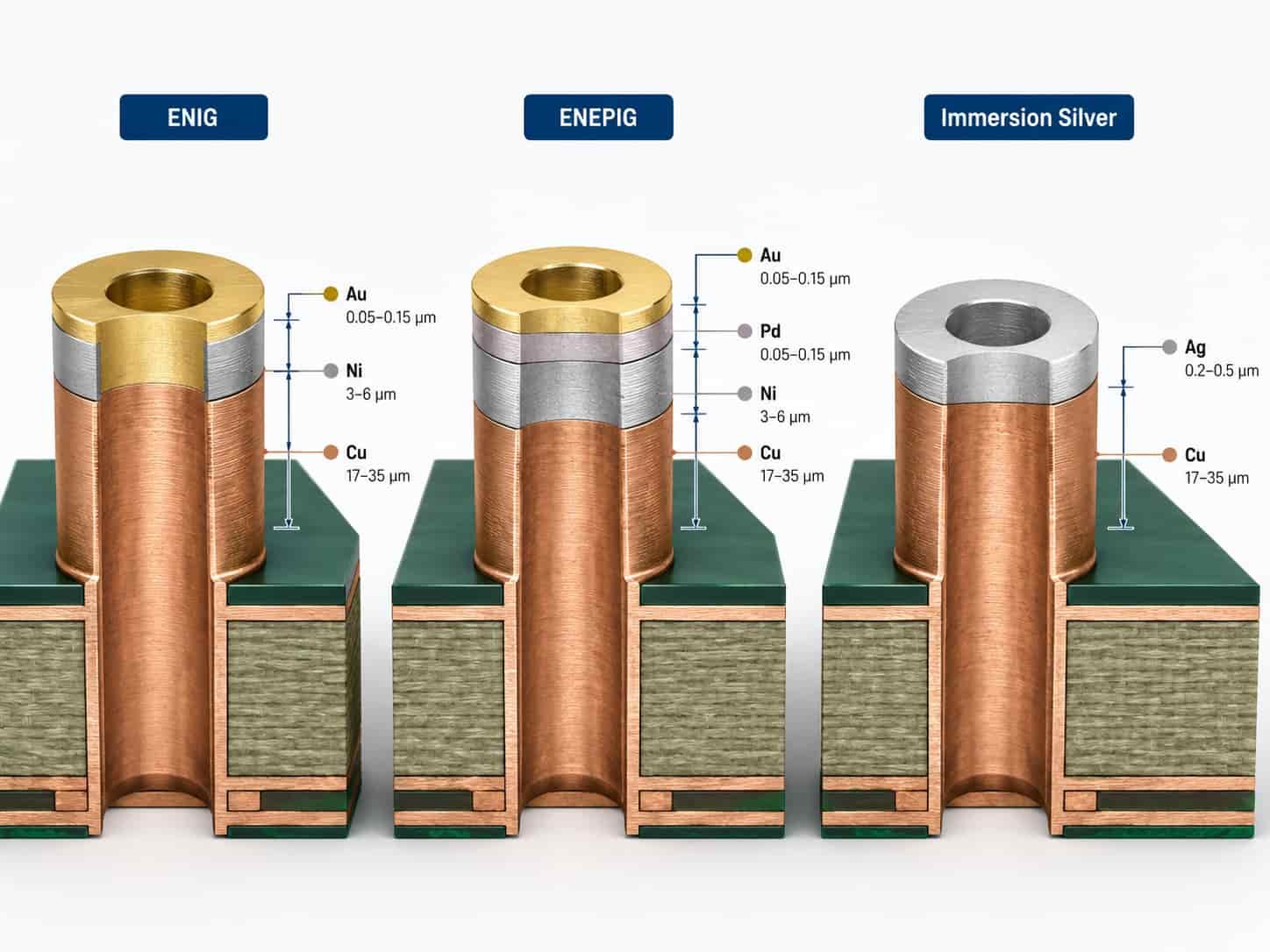
Quick Summary
Key point: ENIG is the most common surface finish for high frequency PCB — flat surface, good solderability, adequate RF performance for most applications up to Ka-band. ENEPIG adds a palladium layer that eliminates the black pad failure risk of ENIG and improves wire bondability — preferred for aerospace and defense high-reliability applications. Immersion silver provides the lowest surface resistance and best RF performance but requires careful handling and storage due to tarnish sensitivity. All three are suitable for lead-free solder assembly.
The right surface finish depends on the assembly process, reliability requirement, operating environment, and RF performance priority of the specific application. Most commercial RF PCB projects specify ENIG. Aerospace and defense programs increasingly specify ENEPIG. Applications requiring the lowest possible RF pad resistance at millimeter-wave frequencies may specify immersion silver.
Layer Structure and Thickness Specifications
Understanding the layer structure of each surface finish is the foundation for comparing their performance. Each finish deposits metallic layers on the copper pad surface in a specific sequence, and each layer has specified thickness ranges that affect RF performance and reliability.
ENIG — Electroless Nickel Immersion Gold
ENIG deposits a nickel barrier layer over the copper pad, followed by a thin immersion gold layer. The nickel provides a flat, solderable surface and protects the copper from oxidation. The gold prevents nickel oxidation and provides the solderable surface that persists through storage and handling.
- Nickel layer: 120–300 µin (3.0–7.6 µm) — barrier between copper and gold, defines pad planarity
- Gold layer: 1–5 µin (0.025–0.127 µm) — thin immersion gold, dissolves into solder during assembly
- Total finish thickness: approximately 3–8 µm above copper pad
- Surface texture: very flat — excellent for fine-pitch components and RF pads
- Color: bright gold appearance
ENEPIG — Electroless Nickel Electroless Palladium Immersion Gold
ENEPIG adds a palladium layer between the nickel and gold of ENIG. The palladium acts as a diffusion barrier that prevents the corrosion mechanism responsible for ENIG black pad failure and also provides a surface suitable for wire bonding — a capability ENIG does not reliably offer.
- Nickel layer: 120–300 µin (3.0–7.6 µm) — same as ENIG
- Palladium layer: 1–2 µin (0.025–0.05 µm) — key differentiator from ENIG; up to 20 µin maximum
- Gold layer: 1–5 µin (0.025–0.127 µm) — same as ENIG
- Total finish thickness: slightly thicker than ENIG due to palladium layer
- Surface texture: flat — comparable to ENIG planarity
- Color: gold appearance, visually similar to ENIG
Immersion Silver
Immersion silver deposits a thin silver layer directly over the copper pad. Silver has the lowest bulk electrical resistivity of any commonly used PCB surface finish metal, which gives it advantages for RF pad performance. However, silver tarnishes in the presence of sulfur compounds and requires careful handling and storage.
- Silver layer: 0.15–0.40 µm (6–16 µin) — thin silver displacement deposit on copper
- No nickel barrier layer — silver deposits directly on copper
- Total finish thickness: very thin — approximately 0.15–0.40 µm above copper
- Surface texture: very flat — similar to ENIG planarity
- Color: bright silver appearance
- Tarnish: tarnishes in air over time — requires controlled storage and short assembly time after opening
Surface Finish Specification Comparison
The table below summarizes the key specifications and characteristics of ENIG, ENEPIG, and immersion silver for high frequency PCB applications.
RF Performance Effects of Surface Finish
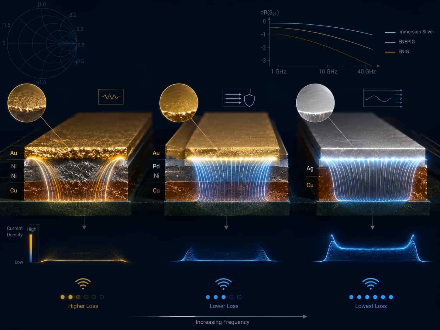
At RF and microwave frequencies, the surface finish layer structure affects signal performance through two mechanisms: skin effect and surface roughness. Understanding these effects helps specify the correct surface finish for demanding millimeter-wave applications.
Skin Effect at Microwave Frequencies
At high frequencies, RF current flows in a thin skin layer at the surface of the conductor. The skin depth decreases as frequency increases — at 10 GHz, the skin depth in copper is approximately 0.66 µm, and in nickel it is much thinner due to nickel’s lower conductivity and higher permeability.
- Copper skin depth at 1 GHz: approximately 2.1 µm
- Copper skin depth at 10 GHz: approximately 0.66 µm
- Copper skin depth at 77 GHz: approximately 0.24 µm
- Nickel conductivity: approximately 14% of copper — much more resistive than copper
- Nickel magnetic permeability: µr ≈ 100–600 — further reduces skin depth in nickel
This means that at frequencies above approximately 1–2 GHz, a significant portion of the RF current flows through the nickel layer of ENIG and ENEPIG rather than the copper. Because nickel is much more resistive than copper, this increases pad resistance and insertion loss compared to a pure copper or silver surface.
ENIG RF Performance
For most RF and microwave applications up to approximately 10–20 GHz, ENIG provides acceptable RF performance. The thin gold layer (1–5 µin) dissolves into solder during assembly, leaving the nickel surface as the RF conductive layer. The nickel contribution to resistance and loss increases with frequency.
- Adequate for most RF applications at L-band through X-band
- Some insertion loss increase at Ka-band and above due to nickel skin effect
- Gold layer too thin to carry RF current — nickel is the effective surface conductor after assembly
- For most defense radar and EW PCB up to X-band: ENIG provides acceptable RF pad performance
ENEPIG RF Performance
ENEPIG RF performance is similar to ENIG at lower microwave frequencies. The palladium layer (1–2 µin) is very thin and does not significantly change the RF current distribution. At millimeter-wave frequencies above 30 GHz, the palladium layer may contribute a small additional resistance compared to ENIG, but the difference is typically small relative to other loss mechanisms.
- RF performance: similar to ENIG at frequencies below Ka-band
- Palladium layer very thin — minimal additional RF resistance vs ENIG in most applications
- Preferred for aerospace and defense over ENIG due to reliability — RF performance trade-off is negligible
- Suitable for all defense radar PCB frequencies including Ka-band and some W-band applications
Immersion Silver RF Performance
Immersion silver provides the best RF pad performance of the three finishes because silver deposits directly on copper with no nickel barrier layer. Silver has nearly the same electrical conductivity as copper, so there is minimal additional resistance or loss from the surface finish layer at any microwave frequency.
- Silver conductivity: approximately 106% of copper — highest of any PCB surface finish metal
- No nickel layer — RF current flows in silver and underlying copper without resistive nickel contribution
- Best RF pad performance at Ka-band, W-band, and millimeter-wave frequencies
- Preferred for lowest-loss RF pad applications — 77GHz automotive radar, W-band EW, mmWave sensing
- Note: tarnished silver has significantly higher resistance — fresh silver surface must be maintained through assembly
Practical guidance: For most high frequency PCB applications below Ka-band, the difference in RF performance between ENIG, ENEPIG, and immersion silver is small enough that the choice is driven by reliability and process requirements rather than RF performance. At Ka-band and above, or in very long feed networks where cumulative insertion loss matters, immersion silver provides a measurable advantage.
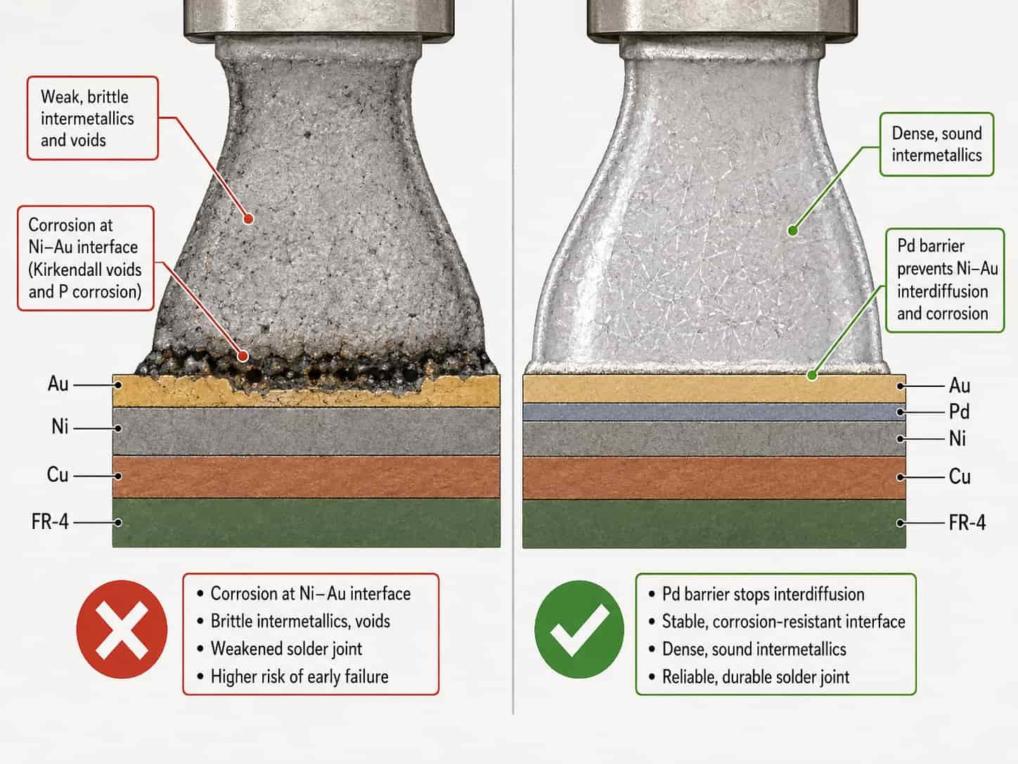
ENIG Black Pad Failure and Why ENEPIG Eliminates It
Black pad is a well-documented failure mode specific to ENIG surface finish. It occurs when corrosion at the nickel-gold interface creates a brittle, phosphorus-rich nickel layer that weakens the solder joint. Components assembled on black pad ENIG pads may pass initial inspection but fail under thermal cycling, vibration, or mechanical stress.
How Black Pad Occurs
During the ENIG process, the immersion gold step deposits gold by displacing nickel atoms from the surface. If this reaction proceeds too aggressively — due to process chemistry imbalance, nickel porosity, or surface contamination — it creates a corrosion layer at the nickel-gold interface. This layer has high phosphorus content, is brittle, and does not wet properly with solder.
- Black pad can occur on any ENIG board — it is not visible before solder assembly
- Detection: typically discovered when a solder joint lifts cleanly from the pad with no solder wetting the nickel
- Risk factors: high phosphorus nickel, aggressive immersion gold chemistry, poor rinse, contaminated bath
- Frequency: relatively uncommon with well-controlled ENIG process, but cannot be fully eliminated
How ENEPIG Eliminates Black Pad
The palladium layer in ENEPIG acts as a complete diffusion barrier between the nickel and the immersion gold step. The palladium prevents the aggressive gold displacement reaction from reaching the nickel surface, eliminating the corrosion mechanism that causes black pad.
- Palladium barrier: completely blocks nickel corrosion during immersion gold step
- Black pad risk: eliminated — ENEPIG has no documented black pad failure mechanism
- Wire bonding: palladium surface supports reliable wire bonding — ENIG does not
- Cost: ENEPIG is approximately 20–40% more expensive than ENIG due to palladium materials and process steps
- Aerospace and defense preference: IPC Class 3 programs increasingly specify ENEPIG to eliminate black pad risk from high-reliability assemblies
Surface Finish Reliability for Aerospace and Defense High Frequency PCB
For aerospace and defense high frequency PCB operating over wide temperature ranges, experiencing thermal cycling, vibration, and long service lives, surface finish reliability is as important as initial RF performance.
ENIG for Aerospace Applications
ENIG is acceptable for many aerospace and defense high frequency PCB applications, particularly where the manufacturing process is well controlled and black pad risk is managed through process audit and incoming inspection. Most commercial and some defense programs continue to specify ENIG for cost reasons.
- Acceptable for most airborne electronics operating at IPC Class 3
- Black pad risk must be managed through process control and supplier qualification
- Not recommended for wire bonded components — use ENEPIG instead
- Thermal cycling: ENIG solder joints on well-wetted pads perform reliably in standard aerospace thermal cycling
ENEPIG for High-Reliability Aerospace and Defense
ENEPIG is increasingly specified for aerospace and defense high frequency PCB where the consequence of solder joint failure is mission-critical. The elimination of black pad risk and wire bonding capability make it the preferred choice for the highest reliability programs.
- Preferred for IPC Class 3 aerospace and defense PCB where zero solder joint defects are required
- Required for wire bonded components — MMIC chips, bare die assembly
- Better resistance to multiple reflow cycles — important for rework and repair in production
- Recommended for programs where field repair is not possible — space-borne, missile, and similar
- Nickel thickness: 120–300 µin — same as ENIG — provides same copper barrier effectiveness
- Gold thickness: 1–5 µin — same as ENIG — same shelf life and storage requirements
Immersion Silver for Aerospace Applications
Immersion silver is used in aerospace applications where its RF performance advantage is needed and where storage and handling can be controlled. Its main limitation for aerospace use is tarnish sensitivity — silver reacts with sulfur compounds in air over time, and tarnished silver has significantly higher resistance.
- Shelf life: typically 6–12 months in sealed dry packaging — shorter than ENIG or ENEPIG
- Handling: requires gloves to prevent skin oil and sulfur contamination
- Assembly: must be assembled within the specified time after opening package
- Conformal coating: compatible with most conformal coatings — coating protects silver from post-assembly tarnish
- Not recommended for programs where bare boards are stored for extended periods before assembly
- Best suited for: Ka-band and W-band radar PCB, 77GHz automotive radar, mmWave sensing PCB requiring minimum pad resistance
Layer Thickness Specifications and Verification
Surface finish layer thickness must be specified on the fabrication drawing and verified by the manufacturer using XRF (X-ray fluorescence) measurement. Correct thickness is critical for both solderability and RF performance.
ENIG Thickness Specification
- Nickel: 120–300 µin (3.0–7.6 µm) — per IPC-4552A, standard range for most applications
- Gold: 1–5 µin (0.025–0.127 µm) — thin immersion gold, dissolves during solder reflow
- Minimum nickel: 120 µin — below this, copper diffusion through nickel may degrade solderability over time
- Maximum gold: 5 µin — gold embrittlement risk above this thickness in tin-lead solder — less concern with lead-free
- Verification: XRF measurement at multiple locations — nickel and gold measured separately
ENEPIG Thickness Specification
- Nickel: 120–300 µin (3.0–7.6 µm) — same as ENIG
- Palladium: 1–2 µin (0.025–0.05 µm) standard, up to 20 µin maximum for wire bonding applications
- Gold: 1–5 µin (0.025–0.127 µm) — same as ENIG
- Palladium verification: XRF measurement — palladium layer must be uniform and continuous
- Wire bonding applications: palladium 4–20 µin for reliable ball bond pull strength
Immersion Silver Thickness Specification
- Silver: 0.15–0.40 µm (6–16 µin) per IPC-4553A
- Minimum silver: 0.15 µm — below this, coverage may be incomplete with gaps in copper protection
- Maximum silver: 0.40 µm — thicker silver may cause silver migration issues in high humidity
- Verification: XRF measurement — silver thickness and coverage uniformity
- Organic solderability preservative (OSP) layer: sometimes applied over immersion silver for extended shelf life
Surface Finish Selection Guide for High Frequency PCB Applications
The following guidance helps select the most appropriate surface finish for common high frequency PCB application types:
Commercial RF PCB — ENIG
- Commercial 5G modules, Wi-Fi, Bluetooth RF front-end: ENIG standard choice
- Industrial RF sensors, commercial radar: ENIG adequate for most applications
- Cost-sensitive programs where black pad risk is acceptable: ENIG
- No wire bonding required: ENIG
Aerospace and Defense High Frequency PCB — ENEPIG
- IPC Class 3 airborne radar, EW systems, navigation PCB: ENEPIG preferred
- Any application with wire-bonded MMIC chips: ENEPIG required
- Programs where field repair is impossible (space, missile): ENEPIG
- High thermal cycling applications (>1000 cycles): ENEPIG recommended
- Long service life programs (>10 years): ENEPIG
Millimeter-Wave and Lowest-Loss RF PCB — Immersion Silver
- 77GHz and 79GHz automotive radar PCB: immersion silver for lowest pad resistance
- W-band (75–110 GHz) defense radar and sensing: immersion silver
- Ka-band phased array where every dB matters: immersion silver
- Applications where boards will be assembled promptly after manufacture: immersion silver
- Conformal coating applied after assembly (protects silver from tarnish): immersion silver
For aerospace and defense high frequency PCB material and reliability requirements, see High Frequency PCB for Aerospace and Defense: Material, Reliability and Manufacturing Requirements. For IPC Class 3 requirements, see IPC Class 3 High Frequency PCB: What It Means for Aerospace and Defense Applications.
Surface Finish Information Needed for High Frequency PCB Quotation
To specify surface finish correctly and support accurate quotation for high frequency PCB, the following information should be included:
- Surface finish type: ENIG, ENEPIG, or immersion silver
- Nickel thickness specification: minimum and maximum (typically 120–300 µin)
- Gold thickness specification: minimum and maximum (typically 1–5 µin)
- Palladium thickness if ENEPIG: standard 1–2 µin, or higher for wire bonding
- Silver thickness if immersion silver: 0.15–0.40 µm per IPC-4553A
- Wire bonding requirement: yes or no — determines palladium thickness for ENEPIG
- IPC-4552A (ENIG), IPC-4552B (ENEPIG), or IPC-4553A (immersion silver) reference standard
- XRF verification requirement: locations and frequency of measurement
- Shelf life and packaging requirement: sealed nitrogen packaging for immersion silver
- Conformal coating compatibility: confirm with coating supplier for immersion silver
- IPC Class requirement: Class 3 for aerospace and defense
For a complete quotation file checklist, see What Files Are Needed for a High Frequency PCB Quotation?.
Conclusion
ENIG, ENEPIG, and immersion silver each address different priorities for high frequency PCB surface finish. ENIG is the practical standard for most commercial RF and microwave PCB applications — cost-effective, flat, and adequate for frequencies up to Ka-band. ENEPIG eliminates the black pad failure risk of ENIG and adds wire bonding capability, making it the preferred choice for IPC Class 3 aerospace and defense programs and any application where solder joint reliability cannot be compromised.
Immersion silver provides the lowest surface resistance and best RF pad performance at millimeter-wave frequencies, but its tarnish sensitivity requires controlled storage and handling. For high frequency PCB projects operating at Ka-band, W-band, or in demanding aerospace and defense environments, specifying the correct surface finish with clear thickness requirements and verification standards is as important as any other PCB parameter.