
GaN RF Power Amplifier PCB — Thermal Via Array, Ground Pad Voids and Material Selection by Power Class
GaN-on-SiC RF power amplifiers pack significantly higher power density into the same package footprint as older LDMOS or GaAs devices, which shifts more of the design burden onto the PCB's thermal path. A QFN-packaged GaN PA that looks electrically identical to a lower-power part on the schematic can require a fundamentally different ground pad via structure underneath it. This guide covers the PCB-side thermal design considerations specific to GaN power amplifiers — via array density by power class, ground pad void control, and material selection. For general RF PA layout and grounding rules that also apply here, see our RF power amplifier PCB design guide.
Home » GaN RF Power Amplifier PCB — Thermal Via Array, Ground Pad Voids and Material Selection by Power Class
Table of Contents
Thermal Via Array and Copper by Power Class
| Output Power Class | Typical Application | Recommended Copper | Thermal Via Density | Substrate Priority |
|---|---|---|---|---|
| ≤5W (small-signal GaN MMIC) | Test equipment, radar exciters | 1–2oz | Standard array, 0.6–0.8mm pitch | RO4350B — adequate |
| 5–15W | EW amplifiers, radar T/R modules | 2oz | Dense array, 0.5mm pitch | RO4350B or TC350 by frequency |
| 15–50W | Radar PA stages, jammer front-ends | 2–3oz | Dense array + backside heatsink coupling | Higher thermal conductivity grade or metal-core hybrid |
| 50W+ | High-power radar, EW transmitters | 3oz+ | Maximum density + direct metal contact | Metal-core or metal-backed hybrid typically required |
The output power class of the GaN device is the primary driver of via array density and copper weight requirements. A 5W part in a small QFN package can often be handled with the same thermal via approach used for general MMIC power amplifiers. Once output power moves into the 15–50W range, standard PCB-only thermal paths often become insufficient on their own, and the design typically needs to work in combination with a backside heatsink or metal-core construction to keep junction temperature within budget.
Ground Pad Void Control
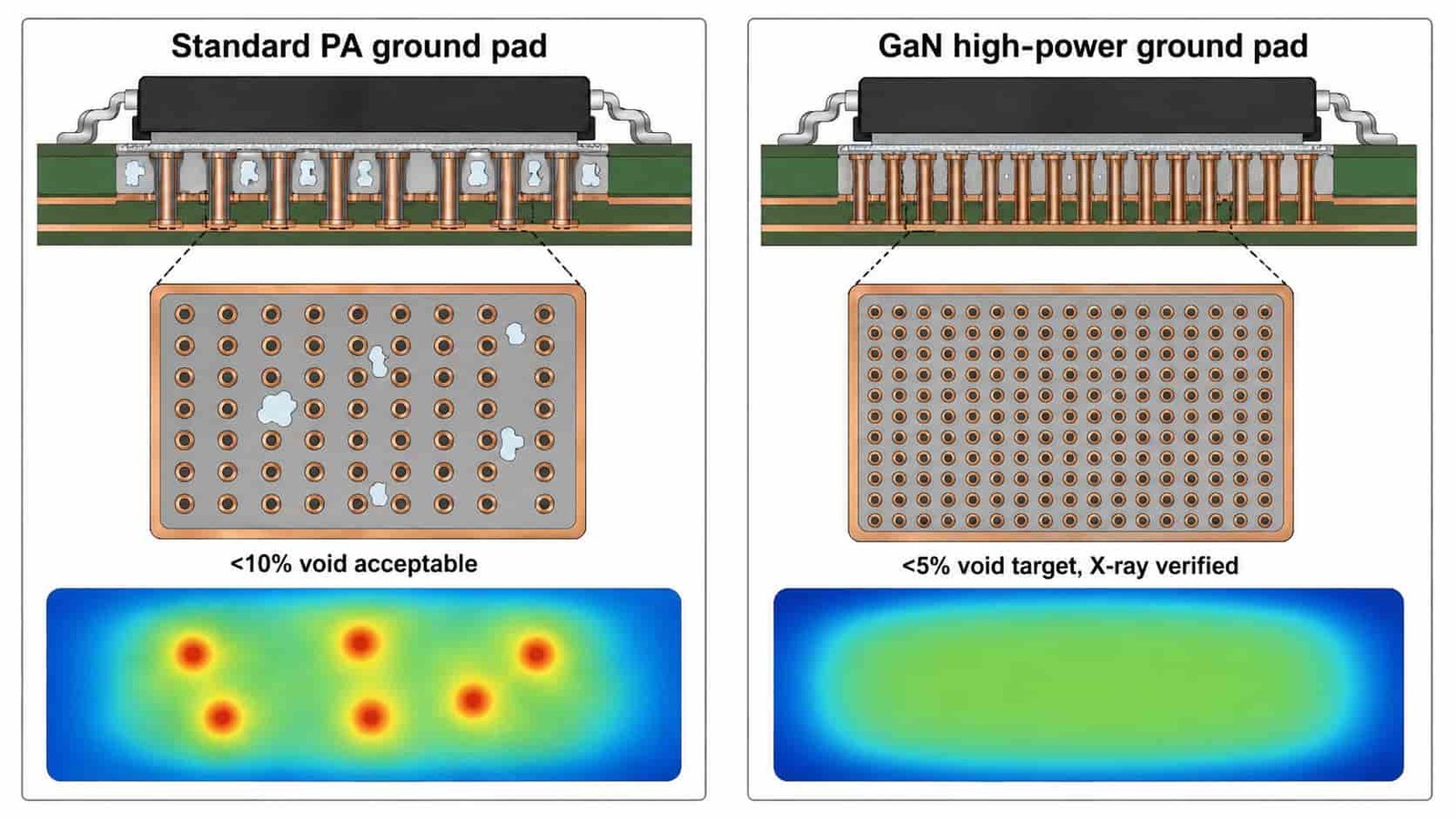
| Parameter | Standard Target | GaN High-Power Target |
|---|---|---|
| Void area per individual via | <10% (IPC Class 2 typical) | <5% — reduces localized hot spots |
| Ground pad void coverage (aggregate) | Not typically specified for standard PA | <10% total void area under die attach pad |
| Via fill type | Open or resin fill acceptable | Copper fill strongly preferred |
| Inspection method | Visual / AOI | X-ray inspection recommended |
Void control under the ground pad matters more for GaN power amplifiers than for lower-power RF devices because voids create localized hot spots directly beneath the highest-power-density area of the die. A via or solder joint with a void does not simply have proportionally reduced thermal performance — heat concentrates around the void, and in a high-power-density GaN device, this local hot spot can meaningfully reduce device lifetime even when the average thermal resistance across the whole pad looks acceptable. For high-power GaN designs, request X-ray inspection of the ground pad via array as a standard quality check, not just for occasional sampling.
Ground Pad Void Control
Ground Pad Void Control
| Material | Dk | Df | Thermal Conductivity | GaN Power Suitability |
|---|---|---|---|---|
| Rogers RO4350B | 3.48 | 0.0037 | 0.69 W/m·K | 5–15W — standard choice below 6GHz |
| Taconic TC350 | 3.5 | 0.0018 | 0.26 W/m·K | Lower thermal — verify against power density |
| Rogers RO3003 | 3.0 | 0.0010 | 0.50 W/m·K | Ka-band GaN PA — moderate thermal |
| Metal-core / metal-backed hybrid | Varies by RF layer | Varies by RF layer | 1.0–3.0+ W/m·K (metal layer) | 25W+ — direct thermal path to heatsink |
Material Dk and Df selection for GaN PA boards follows the same frequency-based rules as any RF power amplifier design — but for GaN specifically, thermal conductivity should be checked against the device’s actual power dissipation, not assumed adequate because a material is commonly used for RF PAs generally. Rogers RO4350B’s 0.69 W/m·K is adequate for many 5–15W designs, but for higher power devices, confirm the junction-to-board thermal path with the device manufacturer’s thermal resistance data before committing to a standard RF laminate alone.
Output Matching Network — Copper Weight and Power Handling
The output matching network on a GaN PA carries significantly higher RF current than the input side, and at higher power levels, trace current-carrying capacity becomes a real constraint alongside impedance matching. Heavier copper (2oz or higher) on the output matching network reduces both resistive loss and localized heating along the trace itself — this is in addition to the thermal via array under the device package, not a substitute for it. Confirm your 50Ω trace width calculation uses the actual copper weight specified, since heavier copper changes the trace width needed for the same target impedance.
Hybrid and Metal-Backed Construction for Higher Power
For GaN devices in the 25W+ range, a PCB-only thermal path — even with an aggressive via array — is often not sufficient on its own. Metal-core or metal-backed hybrid constructions provide a direct low-thermal-resistance path from the RF layer to a heatsink, bypassing the limitations of via-based heat spreading through standard dielectric layers. This is a different construction approach from the RF+FR4 hybrid stackups used for cost optimization — the metal layer here is added specifically for thermal performance, not signal routing.
DFM Checklist for GaN PA PCB
- Confirm thermal via array design against the specific device’s power dissipation and thermal resistance data — do not reuse a via pattern from a lower-power design without recalculating
- Specify copper-filled vias for the ground pad array — resin fill has meaningfully lower thermal conductivity for high-power applications
- Request void inspection (X-ray) as a standard check for the ground pad via array, not just sample inspection
- Confirm output matching network copper weight supports the device’s RF current, separate from thermal via sizing
- For 25W+ devices, evaluate whether metal-core or metal-backed construction is needed before committing to a standard laminate-only stackup
- Confirm ground via inductance is minimized under the package — see via design for RF PCBfor via inductance calculation and its effect on PA stability
GaN RF Power Amplifier PCB Thermal Design — Q&A
Common questions about thermal via arrays, ground pad void control, and material selection for GaN-on-SiC power amplifier PCB.
How is GaN power amplifier PCB thermal design different from standard RF PA design?
GaN-on-SiC devices pack higher power density into the same footprint as LDMOS or GaAs devices, requiring more aggressive via arrays, tighter void control, and copper-filled vias. Above 25W, PCB-only thermal paths often become insufficient and metal-core construction is needed.
What via fill type should be used for GaN PA ground pads?
Copper fill is strongly preferred over resin fill, because copper has meaningfully higher thermal conductivity. This matters more for high-power GaN than standard MMIC applications where resin fill is often acceptable.
Why does void control matter more for GaN PCB than standard RF PA?
Voids create localized hot spots beneath the highest power-density area of the die, reducing device lifetime even when average thermal resistance looks acceptable. Target under 5% void per via and request X-ray inspection as a standard check for high-power GaN designs.
At what power level does GaN PA need metal-core PCB construction?
Generally above approximately 25W, standard laminate-only thermal via arrays are often insufficient. Metal-core or metal-backed hybrid construction provides a direct low-thermal-resistance path to a heatsink, bypassing via-based heat spreading limitations.
GaN PA PCB — Copper-Filled Thermal Via Arrays, X-Ray Void Inspection
Rogers RO4350B and RO3003 in stock. Copper-fill via arrays for high-power ground pads, X-ray void verification available. 2oz–3oz+ copper for output matching networks. Sample to production support.
RF Power Amplifier PCB → WhatsAppRequest a PCB Quote
Upload your Gerber ZIP file and project requirements. Our engineering team will review your PCB material, stackup, impedance needs, surface finish, and production quantity before quoting.
Please prepare:
- Gerber files in ZIP format
- PCB material or stackup requirements
- Controlled impedance notes if available
- Prototype or batch production quantity