High frequency PCB prototypes have longer lead times and more DFM considerations than standard FR4 prototypes. The material availability, PTFE activation process, bonding film requirements, and controlled impedance verification all add steps that a standard FR4 quick-turn service does not have. Understanding what happens between file submission and prototype delivery helps set realistic expectations and avoid the avoidable delays.
As a direct high frequency PCB factory with Rogers, PTFE, Taconic, and F4B materials in production inventory, we produce prototypes from 1 board upward with no minimum order quantity. This guide covers the prototype process from our factory’s perspective.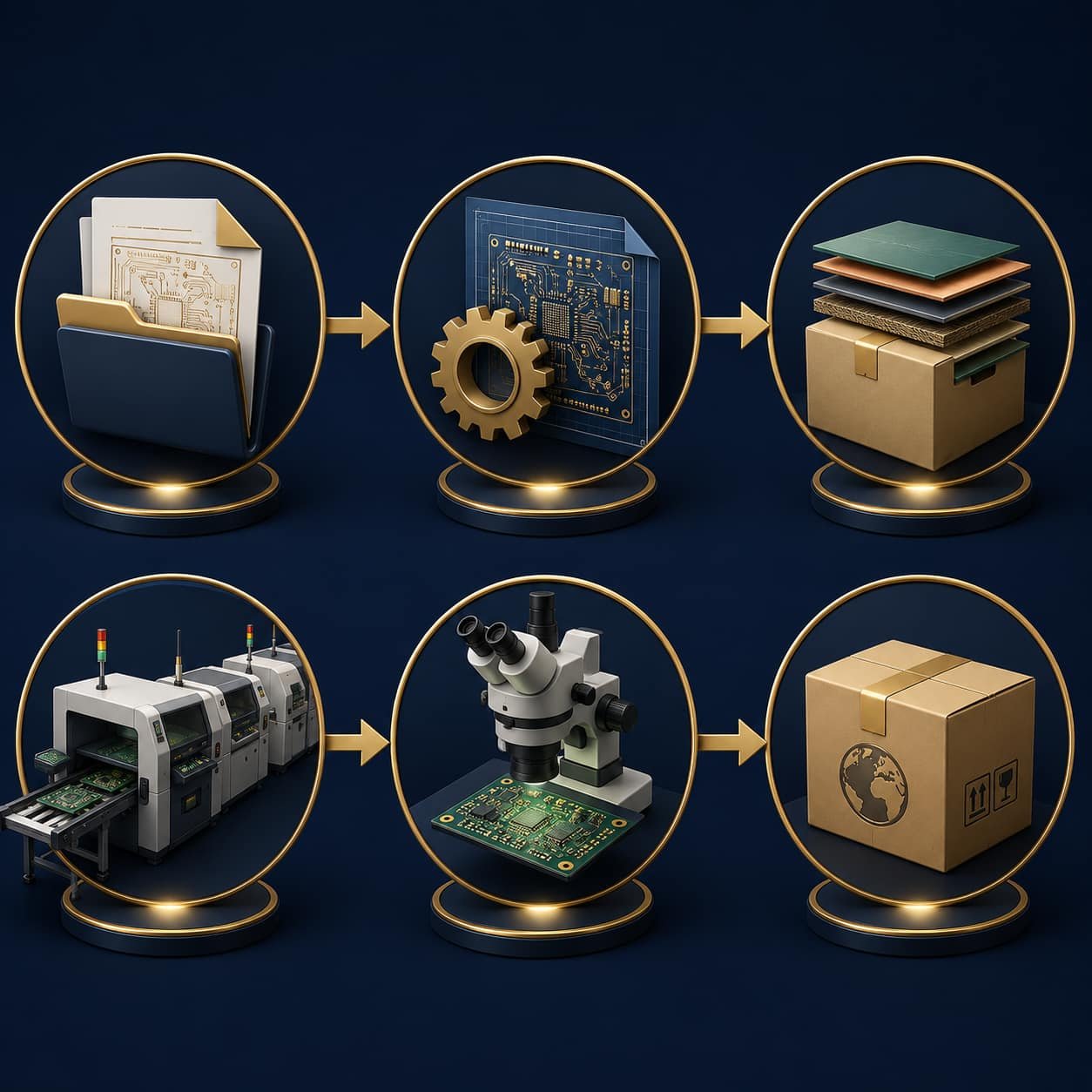
Quick Summary
Lead times at Riching PCB: Rogers RO4350B and RO4003C (2–4 layer, standard): 5–7 working days. Rogers RO3003 and RT5880 PTFE (2–4 layer, standard): 7–10 working days. Complex multilayer (6–12 layer Rogers or hybrid): 10–15 working days. These are standard lead times after DFM review is complete and design is confirmed. Rush options available — contact via WhatsApp +86 13760473650 for specific schedule.
Step 1: File Submission
The prototype process begins with file submission. Complete files allow our engineering team to complete DFM review and confirm the quotation in one pass — incomplete files require back-and-forth and delay the start of production.
What to Submit
- Gerber files: all copper layers, solder mask (top and bottom), silkscreen (if required), board outline
- NC drill file: all hole sizes, PTH and NPTH separated, correct units (mm or inches)
- Stackup drawing: Rogers material grade, dielectric thickness, copper weight per layer — every layer specified
- Controlled impedance: target value, tolerance, layer, transmission line structure
- Surface finish: ENIG, ENEPIG, or immersion silver
- IPC Class: Class 2 or Class 3
- Quantity: number of prototype boards
- Any special requirements: via fill, back drill, conformal coating
Most common missing item: The stackup drawing. Without a complete stackup specifying the Rogers material grade, dielectric thickness, and copper weight for every layer, impedance cannot be calculated and the prototype cannot be quoted accurately. Include the stackup drawing in every submission — it takes 10 minutes to create and saves hours of back-and-forth.
For the complete file checklist, see What Files Are Needed for a High Frequency PCB Quotation?
Step 2: DFM Engineering Review
Every high frequency PCB submission at our factory goes through DFM review by a production engineer before the prototype is confirmed. This is the most important step for avoiding costly first-article failures.
What DFM Review Covers
- Material availability: confirmed Rogers grade and thickness in current inventory
- Bonding film: RO4450F for RO4350B hybrids, Rogers 2929 for PTFE hybrids — confirmed in stock
- Impedance calculation: recalculated using confirmed production Dk from Rogers material certificate lot
- Trace width verification: if specified trace width does not achieve target impedance, correction reported
- Via aspect ratio: every via checked against factory limit for the specified board thickness and material
- Annular ring: checked against IPC Class 2 or Class 3 minimum
- PTFE process confirmation: for RO3003, RT5880, Taconic, F4B — plasma activation confirmed
- Lamination cycle count: for PTFE materials, blind via stages checked against 2-cycle limit
- Board thickness feasibility: total stackup thickness confirmed within tolerance
- Minimum line width: flagged if design has traces below confirmed production capability
DFM Review Turnaround
- Standard Rogers RO4350B 2–4 layer: same day or next business day
- PTFE materials (RO3003, RT5880): 1–2 business days
- Complex multilayer or hybrid: 2–3 business days
- DFM issues found: reported with specific correction recommendations — design may need minor adjustment before production
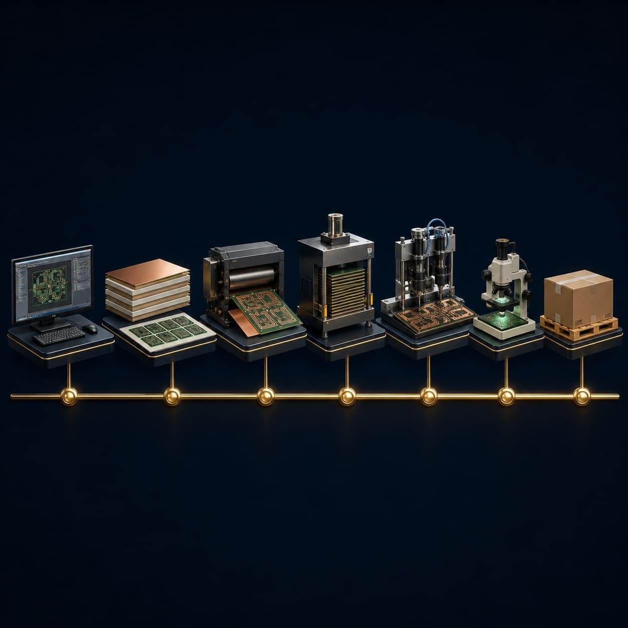
Step 3: Production
After DFM review is complete and the design is confirmed, production begins. The key steps and their sequence:
Rogers RO4350B Prototype — Typical 5–7 Day Production
- Day 1: material cut, inner layer imaging and etching, AOI inspection
- Day 2: lamination (Rogers RO4450F bondply), press cycle
- Day 3: drilling, desmear (standard FR4 process)
- Day 4: electroless copper, pattern plating, outer layer imaging
- Day 5: outer layer etching, solder mask, silkscreen
- Day 6: ENIG surface finish, electrical test, impedance TDR coupon measurement
- Day 7: final inspection, packaging, shipping
Rogers RO3003 PTFE Prototype — Typical 7–10 Day Production
- Same sequence as RO4350B with two additional steps:
- After drilling: plasma activation of PTFE hole walls — adds 0.5–1 day
- Lamination: PTFE-specific press profile — slightly longer than FR4 press cycle
- Total: 7–10 working days for standard 2–4 layer PTFE prototype
Complex Multilayer Hybrid Prototype — 10–15 Days
- Each lamination cycle adds 1–2 days to the production schedule
- Blind via stages: each additional stage adds 2–3 days
- For 6–12 layer Rogers hybrid with blind via: 12–15 working days typical
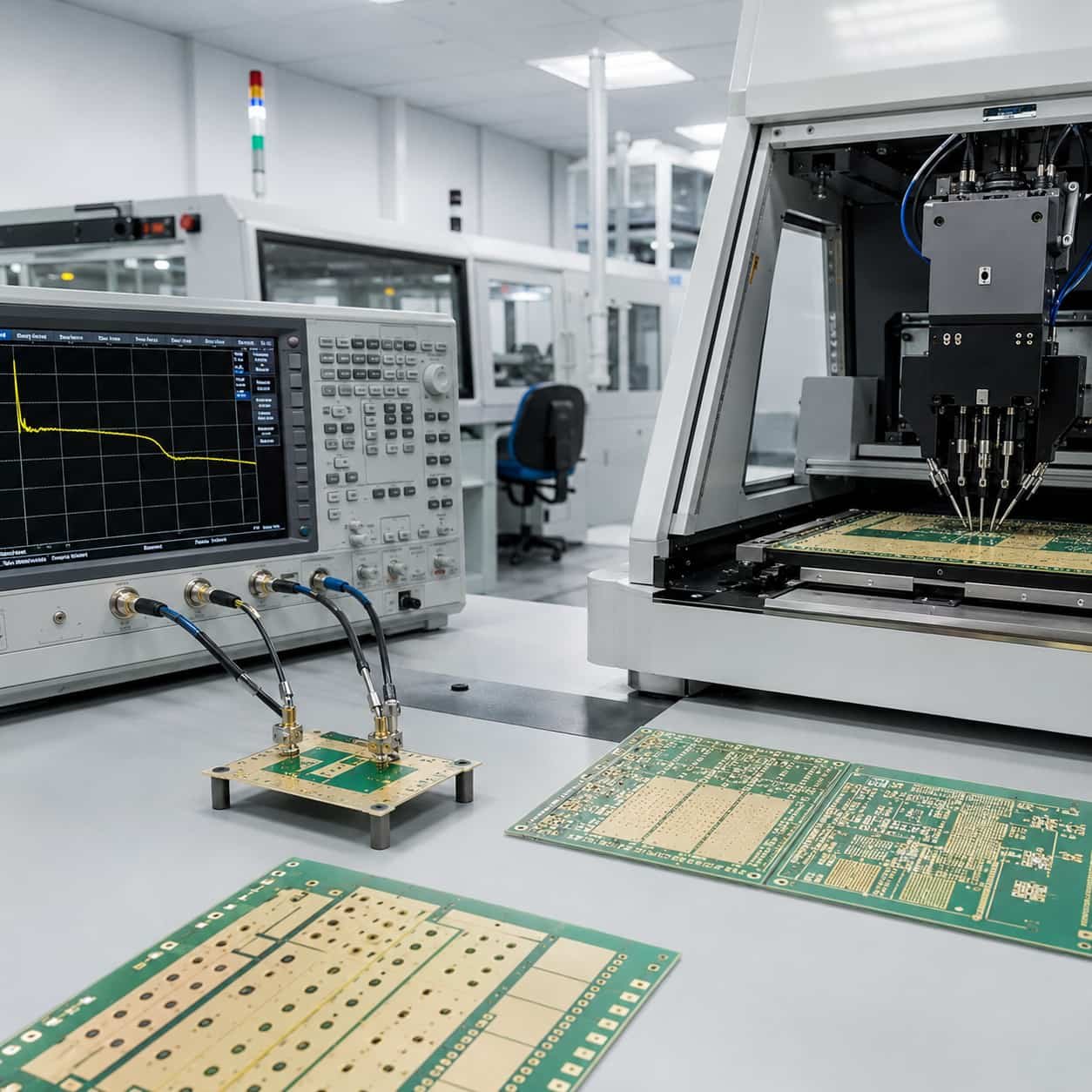
Step 4: Quality Verification
Before a high frequency PCB prototype ships, the following verification steps are completed:
- 100% visual inspection: every board inspected for solder mask, silkscreen, surface finish quality
- 100% electrical test: flying probe test — confirms all nets for continuity and isolation
- Impedance TDR: coupon on panel edge measured — confirms impedance within ±10% or ±8% as specified
- Dimensional check: board outline, hole locations, key dimensions measured
- IPC Class 3 (if specified): microsection FAI, copper plating thickness measurement
- Rogers material certificates: available on request — lot number and confirmed Dk/Df values
What Can Delay a High Frequency PCB Prototype
Understanding the most common delay causes helps set realistic expectations and avoid them:
Delay 1: Incomplete Stackup Drawing
The single most common cause of prototype delay. Without a complete stackup, DFM cannot calculate impedance — we must ask before proceeding. This adds 1–3 days of back-and-forth before production can start.
- Prevention: include complete stackup drawing with every submission
Delay 2: Material Not In Stock
Most standard Rogers grades and thicknesses are in our inventory. Non-standard thicknesses or less common grades may require a material order — adding 3–7 days.
- Prevention: design to standard Rogers thickness ranges — confirm availability before finalizing design
- Standard availability: RO4350B 0.101–1.524mm, RO3003 0.127–1.524mm, RT5880 0.127–3.175mm
Delay 3: DFM Issues Requiring Design Revision
If DFM review finds an issue — trace width incorrect for target impedance, aspect ratio exceeded, wrong bonding film specified — a design correction is needed before production can start. Minor corrections can often be agreed verbally. Major corrections require a revised Gerber submission.
- Prevention: run your own impedance calculation using confirmed Dk before submission — verify trace widths match target impedance
Delay 4: PTFE Material — Additional Process Time
Rogers RO3003, RT5880, Taconic, and F4B PTFE materials require plasma activation and PTFE-specific drill parameters — adding 1–2 days to the production cycle. This is not a problem; it is the correct process.
- Expectation: PTFE prototypes are 2–3 days longer than equivalent RO4350B prototypes
What to Verify When You Receive the Prototype
When the high frequency PCB prototype arrives, the following verification steps confirm manufacturing quality before assembly:
- Visual: check surface finish quality — ENIG gold should be uniform, no bare copper visible
- Dimensional: measure board outline against Gerber — confirm within tolerance (±0.15mm routing)
- Hole check: verify hole count and size match drill file — spot check with pin gauge
- Impedance: if TDR coupon is included, measure yourself and compare against factory record
- Solder mask: check coverage, bridge integrity between fine-pitch pads
- Layer registration: hold board to light and confirm inner layer pads align with outer layer pads
- If IPC Class 3: review microsection report — copper plating minimum 25 µm average
Common Prototype Issues and How to Handle Them
Impedance Out of Tolerance
If TDR measurement on your prototype shows impedance outside the specified tolerance, the root cause is almost always in the stackup — wrong Dk used in calculation, copper weight mismatch, or dielectric thickness variation. Contact the factory with the specific measurement result and the stackup specification. A good direct factory will investigate and confirm the root cause before the production run.
Surface Finish Inconsistency
Minor ENIG color variation between boards is normal. Bare copper spots, rough surface texture, or nickel corrosion (black pad) are not acceptable. Photograph and report to the factory immediately — these are manufacturing defects that should be replaced.
Dimensional Deviation
Board outline deviation within ±0.15mm is within standard tolerance. Larger deviations — holes in wrong location, board significantly smaller or larger than specified — require investigation. Check that Gerber units (mm vs inches) were set correctly in the export — unit confusion is a common cause of dimensional problems.
Prototype Lead Time Summary
How to Order a High Frequency PCB Prototype from Riching PCB
- Send files to WhatsApp: +86 13760473650 — or through richingpcb.com
- Include: Gerber files, NC drill file, complete stackup drawing, impedance requirements, quantity
- DFM review and quotation: same day for standard RO4350B, 1–2 days for PTFE or complex designs
- No minimum order quantity: 1 board prototype orders accepted
- Payment: standard international payment methods accepted
- Shipping: DHL, FedEx, or UPS worldwide — typically 3–5 days to Europe and North America
For complete file submission guidance, see What Files Are Needed for a High Frequency PCB Quotation?. For factory capability overview, see China High Frequency PCB Manufacturer: Rogers, PTFE, Taconic Direct Factory.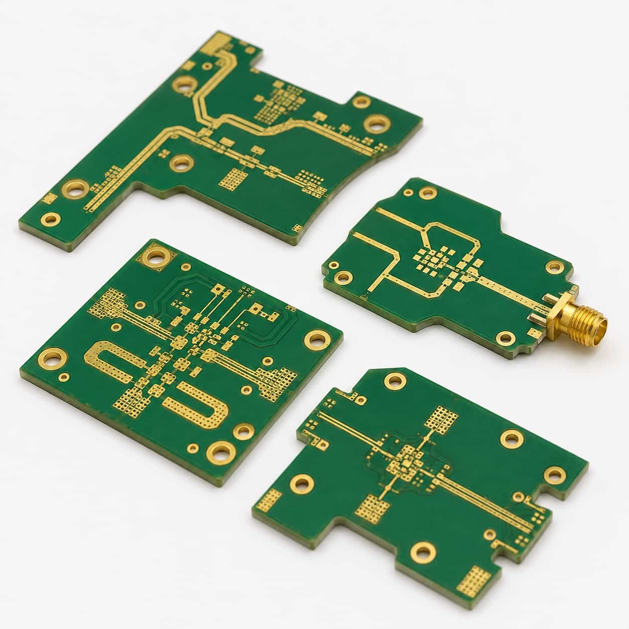
Conclusion
High frequency PCB prototypes take 5–15 working days from complete file submission to shipment, depending on material and layer count. The most common delays are incomplete stackup drawings, non-standard material thickness, and DFM issues requiring minor design corrections. All of these are avoidable with complete file submission and a design that uses standard Rogers thickness ranges.
As a direct high frequency PCB factory with Rogers, PTFE, and Taconic materials in inventory and no minimum order quantity, we produce high frequency PCB prototypes with the same engineering DFM review and TDR impedance verification as production orders. Submit your files and receive a DFM-reviewed quotation from the team that will build the board.