
Microstrip vs Stripline PCB — Loss, Isolation and When Each Structure Wins
Microstrip and stripline are the two fundamental transmission line structures used in RF PCB design — the choice between them affects insertion loss, EMI shielding, trace width, and where in the stackup a signal can physically be routed. This guide compares the two structures on the parameters that determine which one is correct for a given signal path, and covers the practical design rules for each.
Home » Microstrip vs Stripline PCB — Loss, Isolation and When Each Structure Wins
Table of Contents
Structural Comparison
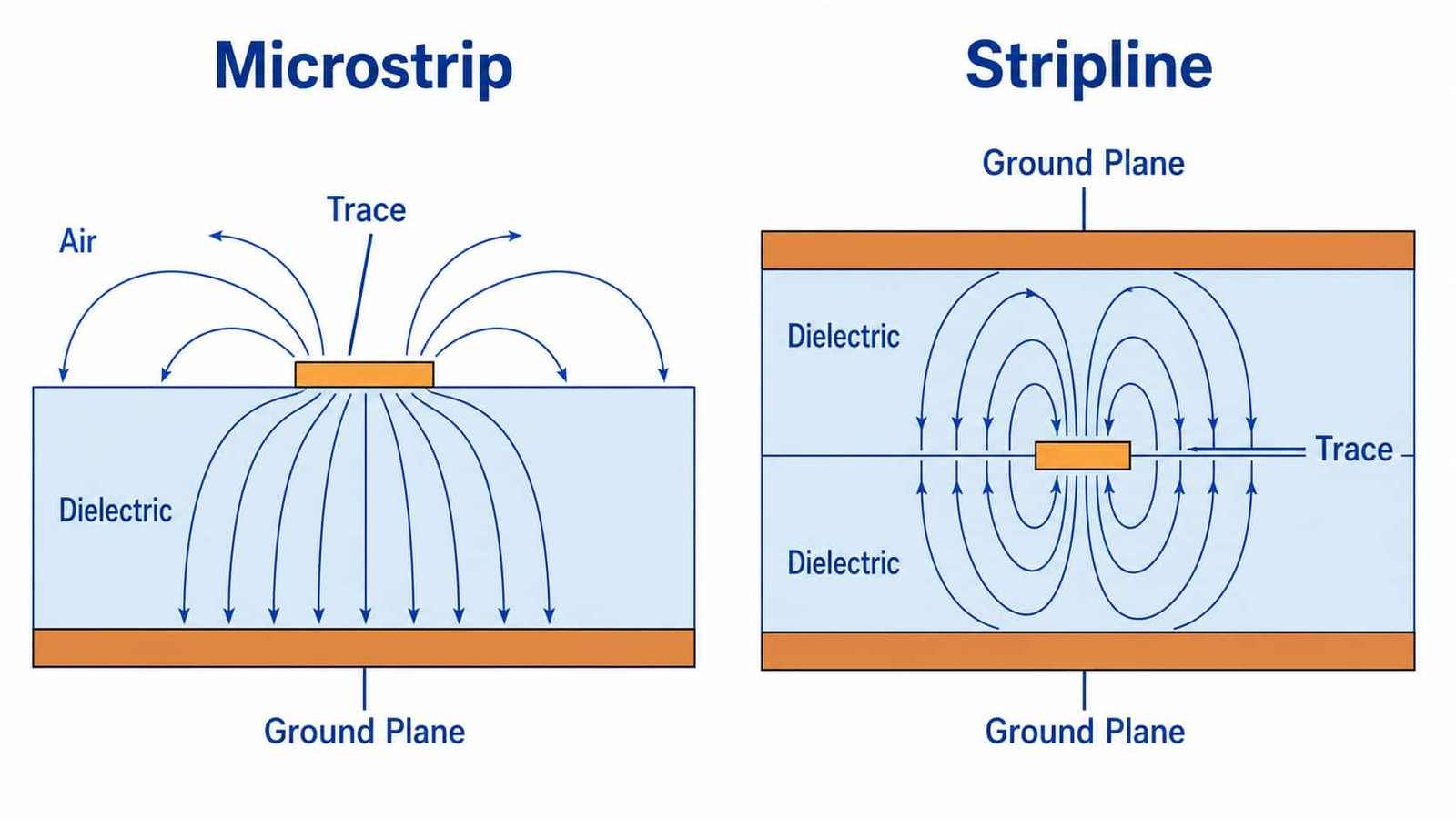
| Factor | Microstrip | Stripline |
|---|---|---|
| Reference planes | One (below the trace) | Two (above and below) |
| Layer position | Outer layer only | Inner layer only |
| Trace width for 50Ω (same Dk, H) | Wider | Narrower — ~half of microstrip |
| Insertion loss (same frequency) | Lower | Higher — trace fully in dielectric |
| EMI shielding | None — exposed, radiates | Excellent — fully enclosed |
| Crosstalk to adjacent circuits | Higher | Lower |
| Component mounting | Direct | Not possible — inner layer |
| Via transition complexity | Simple | More complex — stub management |
| Typical use | Antenna feed, connector launch, tunable filter | High-isolation runs, dense multilayer, EMI-sensitive |
The core structural difference is the number of reference (ground) planes: microstrip has one, positioned directly below the trace with the trace exposed on the outer surface. Stripline has two, with the trace fully embedded between them on an inner layer. This single difference drives every other distinction between the two structures — trace width, loss, shielding, and where in the stackup each can be used.
Trace Width Comparison
| Substrate (Dk 3.48, RO4350B) | Microstrip 50Ω (1oz Cu) | Stripline 50Ω (symmetric, same total H) | Trace Width Ratio |
|---|---|---|---|
| 0.254mm total | ~0.56mm | ~0.28mm | Stripline ~50% narrower |
| 0.508mm total | ~1.05mm | ~0.52mm | Stripline ~50% narrower |
| 0.762mm total | ~1.58mm | ~0.79mm | Stripline ~50% narrower |
For the same total dielectric height and material, stripline requires a trace width roughly half that of microstrip for the same 50Ω impedance target. This is because the stripline trace has ground reference on both sides, concentrating the electric field in a way that produces higher capacitance per unit width — a narrower trace is needed to reach the same characteristic impedance. This narrower trace width is one reason stripline is often the structure of choice in dense multilayer designs where routing space is constrained.
Why Stripline Has Higher Insertion Loss
For the same material and frequency, stripline generally shows higher insertion loss than microstrip. This is because the stripline trace is fully surrounded by dielectric material (contributing dielectric loss on all sides), while microstrip has part of its field in open air above the trace (air has essentially zero dielectric loss). The magnitude of this difference depends on the specific stackup and Df of the material, but it is a consistent directional effect — for loss-critical designs (long feed networks, receiver front-ends where every 0.1dB matters), this tradeoff should be weighed against stripline’s shielding advantage.
EMI Shielding and Crosstalk
Stripline’s two reference planes provide inherent shielding — the trace is enclosed by ground on both sides, preventing radiation from the trace and blocking coupling from adjacent circuits. Microstrip has no shielding above the trace; it radiates more readily and is more susceptible to coupling from nearby traces or external interference. For designs with high channel density or where isolation between specific signal paths is a hard requirement (LNA input separated from PA output, adjacent receiver channels), stripline’s shielding is often the deciding factor even when it comes with a loss penalty.
Which Structure for Which Application
| Application | Recommended Structure | Reason |
|---|---|---|
| Antenna feed line, connector launch | Microstrip | Direct access for tuning, component mounting, connector transition |
| High-isolation signal between sensitive circuits | Stripline | Full shielding from reference planes prevents coupling |
| Dense multilayer routing, EMI-critical design | Stripline (inner layers) | Keeps sensitive signals shielded, frees outer layers |
| Filter requiring physical tuning/trimming | Microstrip | Surface access required for post-fabrication adjustment |
| Via fence / ground isolation critical path | Stripline | Inherent shielding reduces reliance on via fence density |
| Cost-sensitive, simple 2-layer RF board | Microstrip | Simpler stackup, no inner layer routing needed |
Via Transitions Between Microstrip and Stripline
Many designs use both structures — microstrip for connector launches and antenna feeds where surface access is required, stripline for internal routing where isolation matters. The transition between the two, via a through-hole or blind via, introduces an impedance discontinuity and potential via stub resonance if the via passes through unused layers beyond the stripline connection. See via design for RF PCB for via fence and stub management design rules that apply directly at microstrip-to-stripline transitions.
Design Notes for Stripline
- Both reference planes must be continuous beneath and above the stripline trace — any split or gap on either plane creates a return current discontinuity
- Symmetric stripline (trace centered between the two reference planes) is the standard configuration — asymmetric stripline shifts impedance and requires separate calculation
- Confirm impedance using the actual stackup dielectric thicknesses above and below the trace, not a simplified single-dielectric assumption — see controlled impedance PCB design guidefor full impedance specification guidance
- Access for tuning or trimming is not possible on stripline — any post-fabrication adjustment requirement should use microstrip instead
Microstrip vs Stripline PCB — Q&A
Common questions about the structural difference between microstrip and stripline, insertion loss, trace width, and component mounting.
What is the difference between microstrip and stripline?
Microstrip has one reference plane below the trace, exposed on the outer layer. Stripline has two reference planes, fully embedded on an inner layer. Stripline requires a narrower trace, has higher insertion loss, but offers much better EMI shielding and crosstalk isolation.
Which has lower insertion loss, microstrip or stripline?
Microstrip generally has lower loss because part of its field exists in open air (essentially zero dielectric loss), while stripline is fully surrounded by dielectric material. Weigh this against stripline's superior shielding for loss-critical vs isolation-critical designs.
Why is stripline trace width narrower than microstrip for the same impedance?
Stripline has ground reference on both sides, concentrating the electric field and producing higher capacitance per unit width. To reach 50Ω, stripline needs roughly half the trace width of an equivalent microstrip trace for the same total dielectric thickness.
Can I mount components on a stripline trace?
No. Stripline is embedded on an inner layer with no surface access. Any component connection requires transitioning to an outer layer (microstrip) via a through-hole or blind via — this is why microstrip is used for connector launches and antenna feeds.
Microstrip and Stripline — Rogers RO4350B, RO3003, RT5880 In Stock
TDR impedance verification for both structures, ±5% available. DFM review confirms symmetric stripline stackup and layer placement before fabrication. No MOQ.
Controlled Impedance PCB → WhatsAppRequest a PCB Quote
Upload your Gerber ZIP file and project requirements. Our engineering team will review your PCB material, stackup, impedance needs, surface finish, and production quantity before quoting.
Please prepare:
- Gerber files in ZIP format
- PCB material or stackup requirements
- Controlled impedance notes if available
- Prototype or batch production quantity