Microwave PCB signal loss can increase after fabrication when the finished board does not match the electrical assumptions used during design. The problem may come from material change, dielectric thickness variation, copper roughness, trace width deviation, surface finish, via transitions, connector launch, or stackup changes made during production.
For microwave circuits, the PCB is part of the signal path. A board may look clean, pass continuity testing, and still show higher insertion loss during RF measurement. This is why signal loss should be reviewed before fabrication — not only after the prototype returns from the factory.
For buyers, the key is to separate normal manufacturing tolerance from avoidable process risk.
Quick Summary
- Microwave PCBsignal loss may increase because of material substitution, incorrect dielectric thickness, copper roughness, trace width variation, poor connector launch, uncontrolled via transitions, surface finish mismatch, or stackup changes.
- A low-loss laminate alone does not guarantee low-loss performance. The full RF path — including stackup, copper, vias, and connectors — must be reviewed.
- Gerber files alone are not sufficient for serious microwave PCB Stackup, material, impedance, copper thickness, surface finish, working frequency, and application background should all be provided before quotation.
- Prototype results should be linked to a repeatable production stackup if the board will move into batch manufacturing.
Material Was Changed or Not Fully Confirmed
Material selection is the first place to check when signal loss is higher than expected on a microwave PCB.
Some projects begin with one material in the design stage, then shift to another during quotation because of cost, availability, or lead time. That may be acceptable in some cases — but only after a full RF review. Buyers should refer to the Rogers MWI-2021 calculator or the manufacturer’s material comparison data before approving any substitution.
Material change can affect:
- Dk value
- Df value (loss tangent)
- Dielectric thickness
- Copper type
- Copper roughness
- Thermal behavior
- Manufacturing process
- Batch repeatability
For microwave PCB, Df and copper surface condition are especially relevant to signal loss. A material with a similar Dk value may still behave differently in real microwave performance. The design team — not only the purchasing team — should confirm whether a substitute material still meets the loss target and impedance structure.
Dielectric Thickness Shifted From the Design Assumption
Dielectric thickness affects impedance and field distribution. If the manufacturer uses a different laminate thickness or bonding structure from the original design assumption, signal behavior can change.
This may happen when:
- The requested core thickness is not available
- The factory adjusts the stackup to meet final board thickness
- A hybrid stackup is modified during engineering review
- The impedance calculation is rebuilt using different material combinations
- The prototype and batch stackups are not identical
At lower frequencies, a small thickness change may not cause serious problems. In microwave PCB, the same change can affect impedance, insertion loss, and test repeatability. The stackup should be confirmed before production and treated as a fixed RF parameter — not a flexible manufacturing detail. See IPC-2141A for controlled impedance stackup guidelines.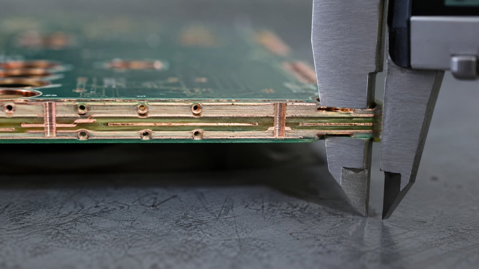
Copper Roughness and Trace Geometry Were Overlooked
Copper is not only a conductor in microwave PCB. Its surface condition and geometry directly influence loss.
At higher frequencies, current tends to flow near the conductor surface — a behavior known as the skin effect. This means copper roughness, trace width, etching quality, and finished copper thickness can all affect RF insertion loss in ways that are not visible during standard inspection.
Manufacturing review should include:
- Copper type
- Copper thickness
- Finished copper thickness after plating
- Trace width tolerance
- Etching compensation
- RF trace length
- Copper roughness specification (if required)
- Panel position and process consistency
A material may be low-loss, but poor copper surface control can still increase total signal loss — especially above 10 GHz.
RF Trace Width Changed During Etching
Microwave transmission lines depend on accurate trace width and spacing. If etching renders a trace narrower or wider than the design value, impedance and loss behavior can shift — sometimes enough to fail the RF test.
This risk is higher when the design includes:
- Long microwave traces
- Narrow controlled impedance lines
- Dense copper patterns near RF paths
- Thicker copper layers
- Tight tolerance requirements
- Fine RF transitions
The manufacturer must understand which traces are RF-critical. If all traces are treated as normal copper routing, the finished board may pass standard inspection but fail microwave PCB performance expectations. Impedance testing per IPC TM-650 should be specified for RF-critical layers.
Via Transitions Added Loss or Reflection
Vias can increase signal loss when used in microwave signal paths without proper review.
A via transition may create discontinuity due to via size, pad size, anti-pad clearance, layer transition length, ground via placement, or via stub length.
Important review points include:
- Signal via diameter
- Via pad size
- Via stub length
- Reference plane connection
- Ground via spacing
- Anti-pad clearance
- Plated through-hole quality
- Layer transition path
If the microwave signal must change layers, the via transition should be designed and manufactured as part of the RF path — not treated as a standard routing convenience. For radar systems and aerospace RF modules, via transitions are often the first place to investigate when measured loss exceeds the simulation result.
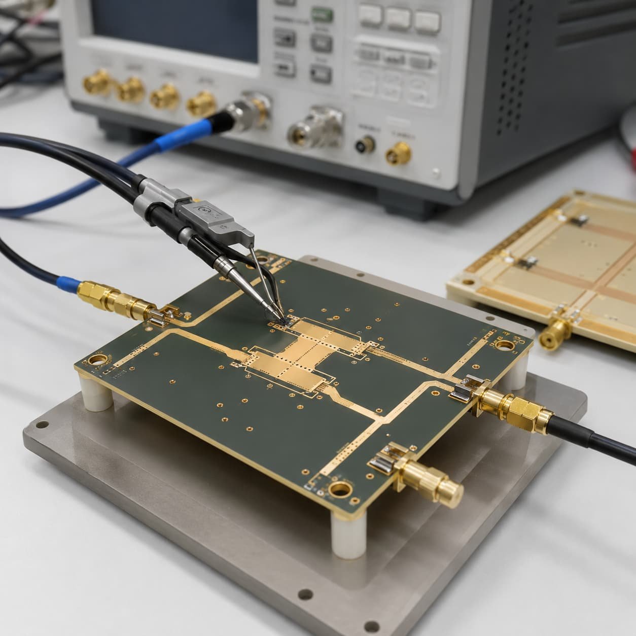
Connector Launch Was Not Controlled
Connector launch areas are common sources of unexpected loss and impedance mismatch.
Even when the PCB trace is correct, signal loss can increase at the transition between RF connector and PCB trace. This is especially common with SMA, SMP, edge launch, or board-to-board RF interfaces on microwave PCB and RF PCB designs.
The review should include:
- Connector footprint accuracy
- Pad-to-trace transition geometry
- Ground via placement
- Reference plane continuity
- Copper clearance
- Mounting hole tolerance
- Surface finish compatibility
- Assembly quality
- Cable stress tolerance
A connector area that looks mechanically correct may still behave poorly at microwave frequencies if the transition geometry is not controlled.
Surface Finish Was Selected by Habit
Surface finish is often chosen from habit, but microwave PCB may need closer review — particularly for exposed RF pads, connector areas, and antenna surfaces.
Common options include:
- ENIG
- Immersion silver
- OSP
- Lead-free HASL
- Hard gold for contact areas
- Customer-specified finishes
ENIG is widely used because it provides flatness and stable solderability. Immersion silver may be considered for RF-sensitive applications where surface conductivity matters. Hard gold may be required for repeated-contact areas.
Surface finish should match the RF path requirement, connector area, assembly process, and storage condition — not simply the default purchasing option.
Prototype and Batch Were Not Built the Same Way
A microwave PCB prototype may pass RF testing, but the batch version may show higher loss if production details change between the two runs.
Common changes that introduce batch variation:
- Different material lot or laminate batch
- Different laminate thickness
- Copper thickness change
- Surface finish change
- Panel layout change
- Connector source change
- Impedance coupon structure change
- Different inspection criteria
The approved prototype stackup should become the fixed reference for repeat production. If the batch order is built using different assumptions, the RF test result may change — particularly for 5G equipment and radar systems where tight loss budgets leave little margin for process variation.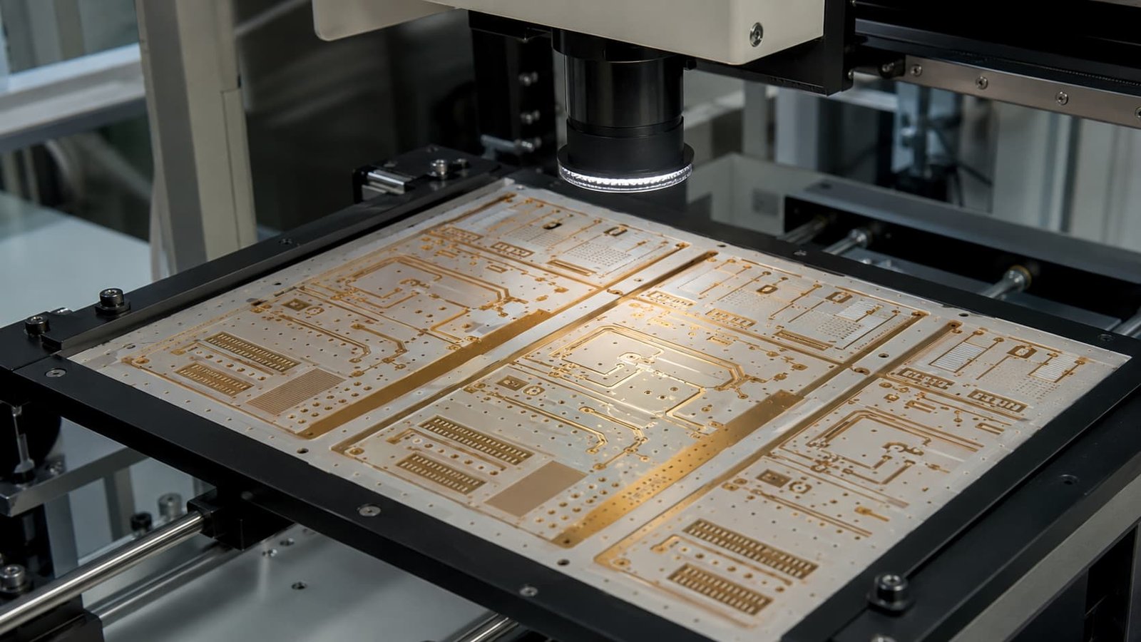
What Buyers Should Provide Before Quotation
To reduce signal loss risk, buyers should prepare a complete quotation package:
- Gerber files
- Drill files
- PCB stackup
- Material requirement
- Working frequency
- Signal loss target (if available)
- Controlled impedance table
- Board thickness
- Copper thickness
- Surface finish
- Connector information
- Quantity
- Prototype or batch plan
- Application background
If the buyer is not yet sure which microwave PCB material or stackup to choose — whether Rogers, PTFE, Taconic, or F4B — working frequency and application background are the most useful starting points for the manufacturer’s review.
Common Mistakes to Avoid
Common mistakes that lead to higher signal loss after fabrication:
- Choosing material based on price alone
- Approving material substitution without RF review
- Sending Gerber files without stackup information
- Ignoring copper roughness requirements
- No controlled impedance table provided
- Treating via transitions as standard routing
- Ignoring connector launch transition geometry
- Selecting surface finish by purchasing habit
- Changing stackup between prototype and batch production
- Not specifying the working frequency
These issues are rarely visible during visual inspection. They typically appear during RF testing, debugging, or repeat production.
Conclusion
Microwave PCB signal loss increases after fabrication when design assumptions and manufacturing reality do not match. Material, dielectric thickness, copper roughness, trace geometry, via transitions, connector launch, surface finish, and production repeatability all affect the final result.
For buyers, a low-loss high-frequency material is only the starting point. The full RF path — from material to copper to vias to connector — must be reviewed before production begins.
A good microwave PCB manufacturer should review stackup, material, impedance, copper condition, via transitions, connector areas, and batch consistency before fabrication starts. That review helps reduce unexpected loss and improves confidence from prototype to repeat production.
For technical reference, see IPC-2141A (Controlled Impedance Circuit Boards), IPC TM-650 (Test Methods Manual), and the Rogers MWI-2021 Impedance Calculator for material selection and loss estimation guidance.