
mmWave Air-Cavity Package to PCB Transition — GCPW Launch and Bond Wire Parasitics
As RF packages push toward 40GHz and above, the transition between the package and the PCB becomes a significant design element in its own right — not just a footprint to route around. Air-cavity QFN packages using wire bond die attach introduce parasitic inductance that must be compensated at the PCB launch, and the launch geometry itself typically shifts from standard microstrip to ground coplanar waveguide (GCPW) at these frequencies. This guide covers the PCB-side design considerations for these transitions. For QFN layout fundamentals at lower frequencies, see our QFN MMIC RF PCB layout guide.
Home » mmWave Air-Cavity Package to PCB Transition — GCPW Launch and Bond Wire Parasitics
Table of Contents
Launch Geometry by Package and Frequency
| Transition Type | Frequency Range | Key Design Factor |
|---|---|---|
| GCPW launch, wire bond package | 20–40GHz | Bond wire length and loop height directly add series inductance |
| GCPW launch, flip-chip/BGA package | 20–60GHz | Shorter, more predictable parasitic path, tighter pad geometry |
| Microstrip launch, wire bond package | 10–24GHz | Simpler transition, less critical compensation below 20GHz |
| Air-cavity package lid clearance | Application-dependent | Cavity height and lid position affect resonance |
Ground coplanar waveguide becomes the standard launch structure at higher mmWave frequencies because it provides tighter field confinement and better isolation than plain microstrip at these dimensions. The ground clearance and center conductor width for GCPW are calculated differently from standard microstrip based on substrate Dk and thickness, so the package manufacturer’s recommended land pattern should be the starting point rather than a generic 50Ω microstrip calculation.
Bond Wire Inductance Compensation
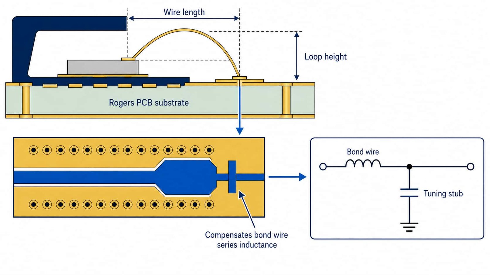
| Bond Wire Parameter | Typical Range | Effect on Transition |
|---|---|---|
| Bond wire diameter | 0.7–1.0 mil (~0.018–0.025mm) | Thinner wire = higher inductance per unit length |
| Bond wire length | 0.3–1.0mm typical | Directly proportional to added series inductance |
| Loop height | 0.1–0.3mm typical | Higher loop increases inductance and radiation |
| Inductance compensation | Capacitive pad/stub tuning | Offsets bond wire inductance, restores 50Ω match |
A bond wire connecting the die to the package lead frame behaves as a series inductor at mmWave frequencies — even a short wire of 0.5mm can present a meaningful reactance at 40GHz. Left uncompensated, this inductance shifts the transition’s impedance away from 50Ω, producing return loss degradation right at the package boundary. The standard compensation technique adds a small capacitive tuning element at the PCB launch pad, sized to offset the bond wire’s series inductance and restore a matched transition. This compensation is package-specific — confirm the recommended launch geometry with the device manufacturer rather than assuming a generic value applies.
Manufacturing Tolerance at the Package Transition
| Parameter | Typical Requirement | Impact if Out of Spec |
|---|---|---|
| Ground via ring pitch around package | ≤λ/10, laser-drilled above 30GHz | Wider spacing leaks energy, degrades isolation |
| Pad position/size tolerance under package | ±0.05mm typical for fine-pitch QFN/BGA | Misalignment affects compensation accuracy |
| Solder mask opening at package footprint | Match datasheet — no default oversizing | Risks bridging on dense RF pad arrays |
| Air-cavity clearance to adjacent structures | Per package datasheet | Can detune the cavity or cause interference |
Ground via ring spacing around the package footprint tightens significantly as frequency increases — a via pattern adequate at 20GHz will likely be insufficient at 40GHz. Confirm your fabricator’s laser drilling capability supports the via density your specific frequency requires before finalizing the footprint, not after Gerber submission.
Air-Cavity Clearance Considerations
Air-cavity packages have an internal cavity above the die that must remain clear of PCB features and adjacent components for correct electrical performance — the cavity geometry is part of the package’s electrical design, not just mechanical clearance. Confirm the package datasheet’s specified keep-out zone around the cavity area, and verify this against your board’s component placement before finalizing layout, particularly for densely populated mmWave modules where adjacent component clearance is often tight.
DFM Checklist for Air-Cavity Package Transitions
- Confirm GCPW ground clearance dimension against the package manufacturer’s recommended land pattern, not a generic microstrip calculation
- Request bond wire length and loop height data from the package manufacturer if you are designing the compensation network yourself
- Confirm ground via ring pitch meets λ/10 at your specific operating frequency — this tightens meaningfully between 20GHz and 40GHz+
- Verify air-cavity keep-out zone against your board’s component placement, particularly for dense mmWave module layouts
- Request a test coupon with the package footprint and launch structure for pre-production verification — see our RF PCB simulation-ready material data guidefor how coupon data closes the loop between simulation and as-built performance
mmWave Air-Cavity Package PCB Transition — Q&A
Common questions about bond wire compensation, GCPW launch geometry, and manufacturing tolerance for high-frequency package transitions.
Why does bond wire length matter for mmWave package transitions?
A bond wire behaves as a series inductor at mmWave frequencies — even a short 0.5mm wire presents meaningful reactance at 40GHz. Uncompensated, this shifts the transition off 50Ω. The fix is a capacitive tuning element at the PCB launch pad.
Why is GCPW used instead of standard microstrip for mmWave package launches?
GCPW provides tighter field confinement and better isolation at mmWave dimensions. Ground clearance and center conductor width are calculated differently from microstrip, so use the package manufacturer's recommended land pattern.
How does ground via ring spacing change between 20GHz and 40GHz designs?
Spacing must stay at or below λ/10. As frequency increases, this tightens significantly — a pattern adequate at 20GHz will likely be insufficient at 40GHz, often requiring laser-drilled microvias.
GCPW Launch and Ground Via Ring Verified Against Package Datasheet
Laser microvia to 0.10mm for tight ground via ring spacing at 40GHz+. Test coupon fabrication with package footprint for pre-production verification. Rogers RO3003, RT5880 in stock.
Free DFM Review → WhatsAppRequest a PCB Quote
Upload your Gerber ZIP file and project requirements. Our engineering team will review your PCB material, stackup, impedance needs, surface finish, and production quantity before quoting.
Please prepare:
- Gerber files in ZIP format
- PCB material or stackup requirements
- Controlled impedance notes if available
- Prototype or batch production quantity