
RF Connector Launch PCB Design — SMA and 2.92mm Transition Rules for Minimum Return Loss
The connector launch — where an RF connector transitions to a PCB microstrip or stripline trace — is one of the most common sources of return loss degradation in an otherwise well-designed RF board. Even a design with correct 50Ω trace geometry and proper via fence isolation along the trace length can show poor return loss if the connector launch itself is not properly designed. This guide covers footprint dimensions for common connector types, ground via placement around the launch, and the trace transition rules that keep the launch impedance matched to 50Ω.
Home » RF Connector Launch PCB Design — SMA and 2.92mm Transition Rules for Minimum Return Loss
Table of Contents
Connector Footprint Reference
| Connector Type | Frequency Range | Center Pin Dia. | Launch Pad Dia. (typ.) | Ground Via Ring Dia. |
|---|---|---|---|---|
| SMA (standard) | DC–18GHz | 1.27mm | ~1.4–1.6mm | ~5–6mm |
| SMA (precision) | DC–26.5GHz | 1.27mm | ~1.4mm | ~5mm |
| 2.92mm (K connector) | DC–40GHz | 0.92mm | ~1.0–1.1mm | ~4mm |
| 2.4mm | DC–50GHz | 0.92mm | ~1.0mm | ~3.5mm |
| 1.85mm (V connector) | DC–67GHz | 0.61mm | ~0.7mm | ~2.8mm |
These dimensions are typical starting points — always confirm exact footprint dimensions against the specific connector manufacturer’s datasheet, as pin diameter and recommended pad geometry vary between manufacturers even for the same connector series (SMA, 2.92mm, etc.). The launch pad diameter directly affects the capacitance at the transition point, which in turn affects impedance matching.
Ground Via Fence Around the Launch
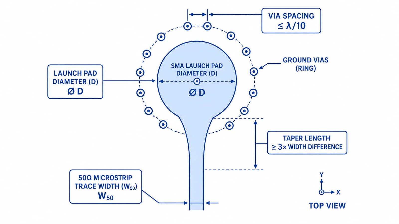
A ring of ground vias surrounding the connector launch pad serves the same function as via fence along a trace: it defines a consistent ground reference and suppresses parallel-plate mode propagation. The spacing rule is the same as for standard via fence — maximum λ/10 at the highest operating frequency. For a design operating at 20GHz, this means via spacing of approximately 1.5mm around the launch; at 40GHz, approximately 0.75mm, generally requiring laser-drilled microvias to achieve.
Trace Transition from Launch Pad to 50Ω Trace
The connector launch pad is typically wider than the 50Ω trace it feeds — this width difference must be tapered gradually rather than stepped abruptly. An abrupt step creates a capacitive discontinuity at that exact point, producing a return loss spike at the frequency where the step dimension becomes electrically significant. The taper length should be at least 3× the width difference between pad and trace — for a pad 1mm wider than the trace, a minimum 3mm taper length.
Material and Frequency Considerations
| Frequency Range | Recommended Connector | Material Consideration |
|---|---|---|
| Below 6GHz | SMA standard | Launch geometry tolerance is forgiving — most materials adequate |
| 6–18GHz | SMA precision | Confirm Dk tolerance — launch pad sizing sensitive to Dk at this range |
| 18–40GHz | 2.92mm (K) | PTFE materials (RO3003, RT5880) typically required — verify launch EM simulation |
| 40GHz+ | 2.4mm or 1.85mm | Thin PTFE substrate (0.127mm) standard — geometry very sensitive to fabrication tolerance |
At frequencies above approximately 20GHz, the connector launch becomes sensitive enough to fabrication tolerance that EM simulation of the specific launch geometry — not just hand-calculated dimensions — is recommended before finalizing layout. See 77GHz radar PCB design guide for via fence and trace geometry considerations that become critical at mmWave frequencies, many of which apply directly to connector launch design at these frequencies.
Design Checklist
| Design Element | Specification |
|---|---|
| Ground via ring around launch pad | Continuous ring, spacing ≤λ/10 at highest operating frequency |
| Ground via to launch pad clearance | ≥connector manufacturer's recommended minimum, typically 0.5–1.0mm |
| Anti-pad on ground layers under launch | Sized to compensate for pad capacitance — confirm with EM simulation above 20GHz |
| Trace width taper | Gradual taper length ≥3× the width difference — avoid abrupt step |
| Solder mask relief | Keep mask clear of the connector footprint and adjacent trace |
| Board edge clearance | Per connector datasheet — typically specific edge overhang or flush mount dimension |
RF Connector Launch PCB Design — Q&A
Common questions about connector footprint dimensions, ground via spacing, trace taper and connector selection by frequency.
What is a connector launch in RF PCB design?
The transition point where an RF connector connects to a PCB trace. It's a common source of return loss degradation — the connector's pin geometry and pad create an impedance discontinuity requiring careful ground via placement, pad dimensions, and trace taper.
What ground via spacing is needed around an RF connector launch?
Same rule as standard via fence: max λ/10 at highest operating frequency. At 20GHz, ~1.5mm spacing; at 40GHz, ~0.75mm, typically requiring laser-drilled microvias.
Why does the trace need to taper at a connector launch pad?
The launch pad is typically wider than the 50Ω trace. An abrupt width step creates a capacitive discontinuity causing a return loss spike. Taper should be at least 3x the width difference — for a pad 1mm wider, minimum 3mm taper length.
Which connector type should I use above 18GHz?
2.92mm (K) connector is standard for 18-40GHz, rated to DC-40GHz. Above 40GHz, 2.4mm (to 50GHz) or 1.85mm (to 67GHz) connectors are used, generally with thin PTFE substrate (0.127mm).
Connector Launch Review Included in Every DFM Check
SMA, 2.92mm and higher-frequency connector footprints verified against ground via spacing and impedance target before fabrication starts. Laser microvia to 0.10mm for tight via fence spacing. Free DFM review, no MOQ.
Free DFM Review → WhatsAppRequest a PCB Quote
Upload your Gerber ZIP file and project requirements. Our engineering team will review your PCB material, stackup, impedance needs, surface finish, and production quantity before quoting.
Please prepare:
- Gerber files in ZIP format
- PCB material or stackup requirements
- Controlled impedance notes if available
- Prototype or batch production quantity