
RF PCB layout review should happen before the board enters production, not after the first prototype fails RF testing. In high frequency circuits, the PCB layout affects more than electrical connection. RF traces, ground planes, vias, connector areas, antenna keep-out zones, and stackup details all influence signal behavior.
For a standard control board, a layout issue may be easy to fix in the next revision. For an RF PCB, a small routing or grounding problem can affect impedance matching, signal loss, antenna efficiency, or test repeatability.
That is why RF layout review is a practical step for RF PCB manufacturing, microwave PCB manufacturing, antenna PCB manufacturing, and high frequency PCB projects.
Infineon’s official Antenna Design and RF Layout Guidelines covers RF trace, PCB stackup, via holes, antenna grounding, decoupling, and antenna tuning considerations, which are all relevant during layout review.
Quick Summary
RF PCB layout review should check RF trace routing, controlled impedance, ground reference, via placement, antenna clearance, connector transitions, stackup, copper thickness, and surface finish.
The most common layout risks are broken ground reference, uncontrolled RF trace width, poor via transitions, weak grounding, antenna keep-out violations, and missing impedance information.
For wireless modules, antenna PCBs, radar boards, and microwave circuits, the layout should be reviewed together with the stackup and material choice.
A good RF PCB manufacturing review should include Gerber files, drill files, stackup, impedance table, material requirement, working frequency, and application background.
Check the RF Trace First
The RF trace is usually the first place to review.
RF traces should not be treated like normal copper routing. Their width, length, spacing, and reference plane all matter. If the trace was designed as a 50-ohm line, the manufacturer needs to confirm whether the real stackup can support that impedance.
A layout review should check:
RF trace width
Trace spacing
Trace length
Reference ground plane
Copper thickness
Solder mask condition
Connector transition
Component pad transition
Sharp bends or unnecessary discontinuities
Analog Devices’ RF and mixed-signal PCB layout guidance recommends keeping RF transmission lines apart where possible and using a ground plane between crossing lines on separate layers. This is a useful reminder that RF layout is about field behavior, not only copper connection.
Confirm the Ground Reference
A stable ground reference is one of the easiest things to overlook.
If the RF trace loses its ground reference, impedance can shift and return current may take an unwanted path. This can create radiation, coupling, noise, or unstable RF test results.
During layout review, check whether:
The ground plane is continuous under RF traces
There are no unnecessary splits under RF paths
Ground vias are placed near connectors and RF transitions
The RF return path is short and predictable
Shielding areas have enough ground connection
Antenna keep-out zones are respected
For many projects, weak grounding causes more problems than the laminate itself. A good material cannot save a layout with a broken return path.
Review Controlled Impedance Against the Real Stackup
Controlled impedance is only useful if it matches the real manufacturing stackup.
The impedance calculation should use actual material Dk, dielectric thickness, copper thickness, trace width, reference plane structure, and solder mask condition. If the design file assumes one stackup but production uses another, the finished board may not match the intended RF performance.
For this reason, RF layout review should happen together with RF PCB stackup design and controlled impedance RF PCB review.
The quotation package should clearly state:
Target impedance
Tolerance requirement
Layer location
Trace structure
Reference plane
Test coupon requirement if needed
If these details are missing, the PCB may be quoted and produced as a normal board instead of a controlled impedance RF board.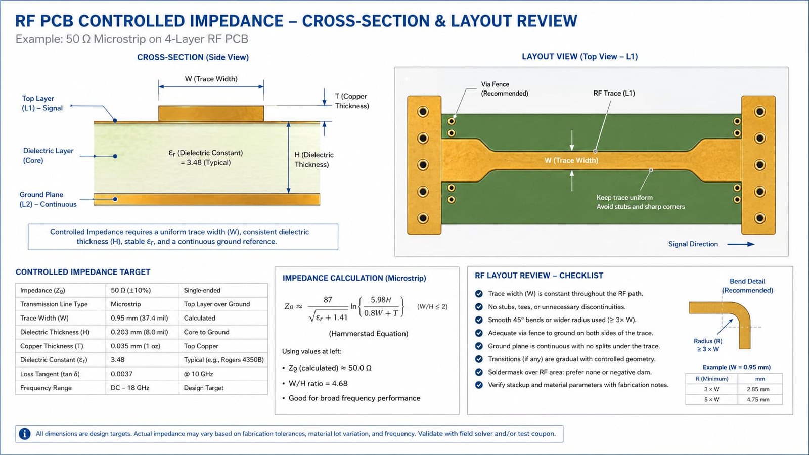
Check Vias and Layer Transitions
Vias can be useful, but they can also create problems.
In RF PCB layout, vias may be used for signal transitions, ground connections, via fences, connector grounding, shielding, or thermal paths. The risk is that every via adds geometry. At high frequency, geometry becomes electrical behavior.
A layout review should check:
Signal via position
Ground vias around RF transitions
Via stub length
Anti-pad size
Ground via fence spacing
Connector via placement
Via distance from antenna traces
Plated through-hole reliability
Protect the Antenna Area
Antenna layout needs its own review.
Antenna performance can be affected by copper, ground, components, battery position, cables, screws, shielding cans, and housing materials. A PCB antenna or antenna feed line should not be checked only as a copper pattern. It should be reviewed as part of the RF system.
Texas Instruments’ Antenna Selection Guide notes that antenna size, cost, and performance are important factors when choosing antenna types for short-range devices.
For antenna PCB layout review, check:
Antenna keep-out area
Feed line impedance
Ground clearance
Matching circuit placement
Nearby copper and components
Connector location
Board edge position
Mechanical environment
For wireless device projects, antenna PCB manufacturing and Antenna PCB for Wireless Devices should be reviewed together with layout and material selection.
Check RF Connectors and Launch Areas
RF connector launch areas are common sources of performance problems.
A connector footprint may look correct mechanically but still create an RF discontinuity if the ground vias, pad transition, trace width, and reference plane are not handled properly.
Review these points:
Connector footprint
Pad-to-trace transition
Ground via placement
Reference plane continuity
Copper clearance
Mechanical hole tolerance
Surface finish requirement
Assembly process
For test boards, antennas, radar modules, and microwave circuits, the connector area often deserves extra attention because it is where the signal enters or leaves the PCB.
Review Material and Layout Together
RF layout cannot be separated from material choice.
A layout designed for one material may not behave the same way if the laminate changes. Dk, Df, dielectric thickness, copper type, and thickness tolerance all affect impedance and loss.
Common high frequency material options include:
Rogers materials
PTFE laminates
Taconic materials
F4B materials
FR4 plus high frequency hybrid stackups
For material-side review, Riching PCB’s pages on Rogers materials, PTFE PCB manufacturing, Taconic materials, and F4B materials can support different RF and microwave PCB requirements.
Keep the Layout Manufacturable
A good RF layout still needs to be manufacturable.
Before production, the manufacturer should check whether the design can be built with reliable tolerances. Very narrow traces, tight spacing, dense vias, thin dielectric layers, or complex hybrid stackups can increase risk.
Layout manufacturability review should include:
Minimum trace width and spacing
Copper thickness
Etching tolerance
Drill size
Via structure
Layer registration
Surface finish
Board thickness
Panelization
Final inspection requirement
This is also why buyers should send complete files, not just screenshots or partial Gerber data. A proper quote needs Gerber files, drill files, stackup, material requirement, impedance details, quantity, and working frequency.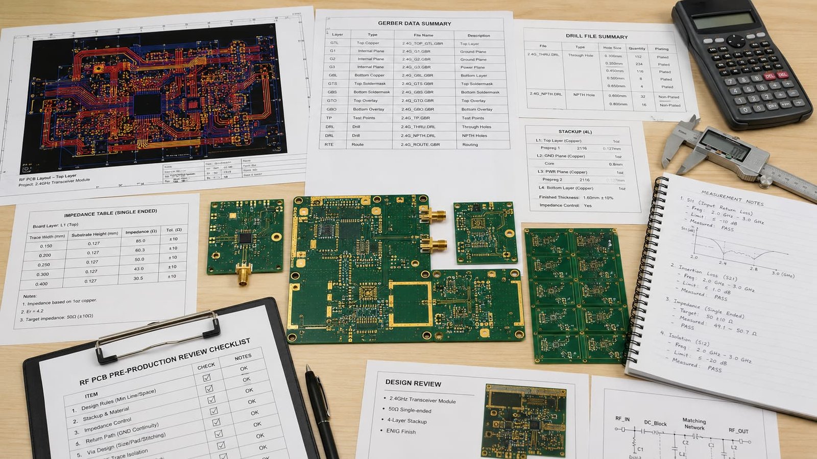
Common RF Layout Problems Before Manufacturing
The most common RF layout problems are not always dramatic. Many are small details that only become visible during testing.
Common issues include:
RF trace width does not match stackup
Ground plane is broken under RF path
Too few ground vias near connector
Via stubs are ignored
Antenna keep-out area is violated
Matching circuit is too far from antenna feed
Material is changed without impedance review
Surface finish is selected only by habit
No working frequency is provided
No impedance table is included
These problems slow down quotation, production review, and prototype debugging.
Conclusion
RF PCB layout review is a manufacturing step, not only a design step. Before production, the layout should be checked for RF trace routing, ground reference, controlled impedance, via transitions, antenna areas, connector launches, material choice, and manufacturability.
For RF modules, microwave circuits, antenna PCBs, radar boards, 5G communication devices, and high frequency test boards, early layout review can reduce prototype failures and improve batch consistency.
A good RF PCB project starts with complete files, a clear stackup, known material requirements, and enough RF context for the manufacturer to review the board before fabrication.