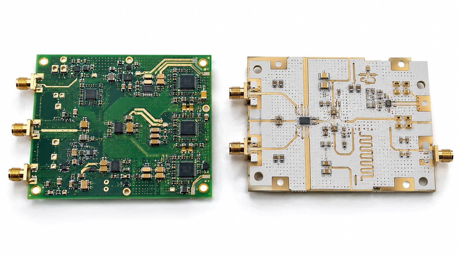
RF PCB and microwave PCB are both used for high frequency signal applications, but they are not always the same thing. RF PCB is a broader term for circuit boards used in radio frequency applications, while microwave PCB usually refers to boards working at higher frequency ranges where signal loss, dielectric stability, stackup accuracy, and manufacturing tolerance become more sensitive.
For buyers, the difference matters because material choice, impedance control, drilling, vias, surface finish, and inspection requirements may change as frequency increases. A board that works well as an RF PCB may not automatically meet the requirements of a microwave circuit.
The safest way to compare them is not by name. It is to review the working frequency, signal loss target, transmission line length, controlled impedance requirement, stackup, material system, and production quantity before quoting or manufacturing.
Quick Summary
RF PCB is a general term for circuit boards used in radio frequency applications, including wireless modules, antenna circuits, RF front-end boards, industrial RF devices, and communication equipment.
Microwave PCB usually works at higher frequencies and often needs lower-loss materials, tighter impedance control, more careful stackup review, and stronger manufacturing consistency.
Both RF PCB and microwave PCB may use Rogers, PTFE, Taconic, F4B, FR4 hybrid, or other high frequency materials depending on the design requirement.
The main difference is not only frequency. Microwave PCB projects usually leave less room for casual material substitution, stackup changes, uncontrolled vias, or loose manufacturing tolerance.
RF PCB: The Broader Category
RF PCB covers a wide range of radio frequency circuit boards.
Typical RF PCB applications include:
Wireless communication modules
Bluetooth and WiFi devices
IoT wireless boards
RF front-end modules
Antenna feed circuits
RF amplifiers
Remote control systems
Industrial RF equipment
Communication devices
Test boards
Some RF PCB projects may work at relatively moderate frequencies. In these cases, the design may still need controlled impedance and careful grounding, but the material choice may have more flexibility.
For example, some RF boards may use standard FR4 if the frequency and signal loss requirement are not too demanding. Other RF boards may require Rogers, PTFE, Taconic, F4B, or hybrid stackups when the signal path is more sensitive.
Microwave PCB: Less Tolerance for Mistakes
Common microwave PCB applications include:
Radar electronics
Satellite communication boards
High frequency antenna systems
RF test equipment
Microwave filters
High-speed signal transmission boards
Aerospace RF circuits
At microwave frequencies, small manufacturing changes can become visible in testing. A slight change in dielectric thickness, trace width, copper thickness, or via structure may shift impedance or increase loss.
This is why microwave PCB projects usually need more careful review before production. The manufacturer should not treat them as normal PCB orders with a special material name.
Frequency Is Only the Starting Point
Many people try to separate RF PCB and microwave PCB only by frequency. That helps, but it is not enough.
Two boards may work in similar frequency ranges but have very different manufacturing requirements. A short RF trace inside a compact module may be easier to control than a long microwave signal path with strict loss requirements. An antenna board may be more sensitive to material thickness than a small RF control board.
The real review should include:
Working frequency
Signal path length
Insertion loss requirement
Impedance target
Antenna or non-antenna design
Layer count
Board thickness
Copper thickness
Material availability
Prototype and batch quantity
This is why buyers should provide application background, not only Gerber files.
Material Selection
Material selection is one of the biggest differences between general RF PCB and microwave PCB.
For lower-risk RF applications, the material may be selected based on cost, availability, and basic impedance needs. For microwave applications, material Dk, Df, thickness tolerance, copper type, and signal loss behavior need closer review.
Common material options include:
FR4 for less demanding RF sections
Rogers materials for RF and microwave performance
PTFE laminates for low-loss microwave circuits
Taconic materials for RF and microwave boards
F4B materials for balanced performance and cost
Hybrid stackups for mixed RF and digital functions
A buyer should avoid writing only “high frequency material accepted.” That gives the manufacturer too much room for assumptions. A better quotation request includes the expected material, working frequency, impedance requirement, and production target.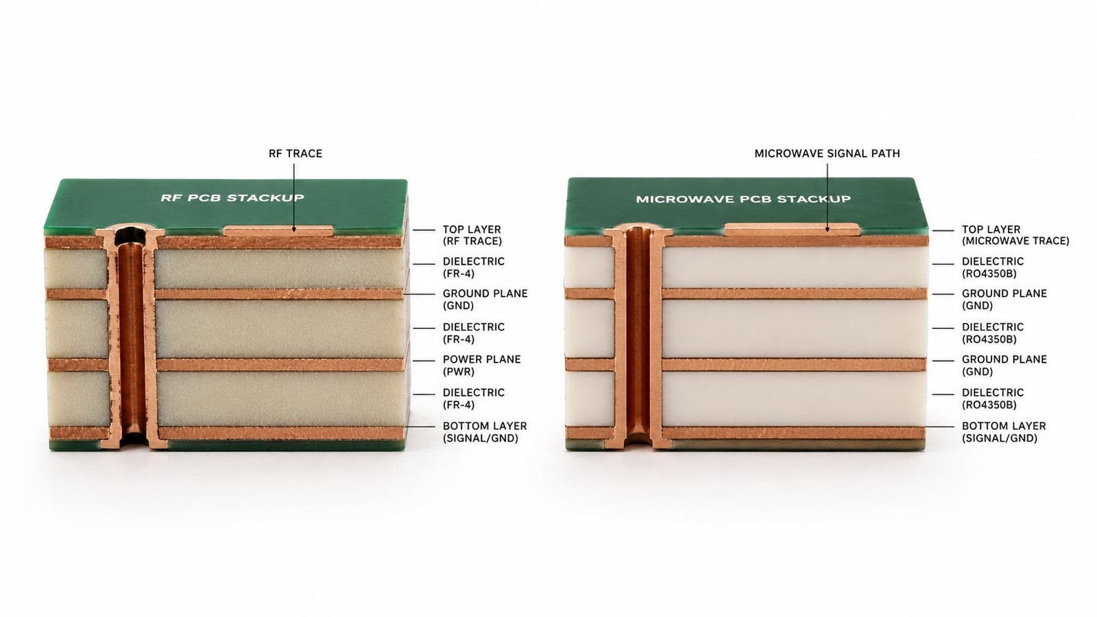
Stackup and Controlled Impedance
Both RF PCB and microwave PCB may require controlled impedance, but microwave PCB usually gives the manufacturer less room for adjustment.
Controlled impedance depends on:
Material Dk
Dielectric thickness
Trace width
Copper thickness
Ground reference
Solder mask condition
Etching tolerance
Final production stackup
If the design assumes one stackup and production uses another, the finished board may not behave as expected. This is especially risky in microwave PCB projects because impedance shift and signal loss may become more obvious.
For RF PCB, some designs may tolerate small differences. For microwave PCB, the stackup should be confirmed before production and should not be changed casually after impedance calculation.
Layout and Grounding
RF layout and microwave layout both need clean signal routing and stable ground reference.
The review should check:
RF trace width and spacing
Ground plane continuity
Via placement
Connector transition
Return path
Antenna keep-out area
Shielding areas
Crosstalk risk
Component pad transition
Microwave PCB layout is usually more sensitive to discontinuities. Poor connector launches, long via stubs, broken ground planes, or uncontrolled trace transitions can create signal reflection or extra loss.
A good material cannot fully compensate for poor layout. If the RF path is badly designed, even a premium laminate may not solve the problem.
Vias and Plated Through Holes
Vias become more sensitive as frequency increases.
In RF PCB, vias may be used for grounding, layer transitions, connector pads, or via fences. In microwave PCB, the same via structure may need deeper review because via length, pad size, anti-pad clearance, and stub behavior can affect performance.
Important via points include:
Signal via size
Ground via spacing
Via stub length
Connector grounding
Via fence design
Plated through-hole reliability
Layer transition structure
Hole wall quality
For multilayer microwave PCB, via review should happen before manufacturing. If the board is already fabricated, via-related RF problems are difficult to correct without redesign.
Surface Finish
Surface finish should match the application and assembly process.
Common options include:
ENIG
Immersion silver
OSP
HASL
Lead-free HASL
Hard gold for contact areas
Customer-specified finishes
For many RF PCB projects, ENIG is a practical and widely used finish because it provides a flat surface and stable solderability. For some microwave applications, immersion silver may be reviewed when surface conductivity and RF-sensitive areas matter.
Surface finish is not usually the first factor in impedance calculation, but it can still affect connector areas, RF pads, soldering quality, bonding requirements, and storage reliability.
Manufacturing Review
RF PCB and microwave PCB both need engineering review, but microwave PCB usually needs a stricter check before release to production.
A good manufacturing review should include:
Gerber files
Drill files
PCB stackup
Material requirement
Working frequency
Impedance table
Copper thickness
Board thickness
Surface finish
Via structure
Quantity
Application background
For RF PCB, the main risk may be impedance mismatch, grounding, or material choice. For microwave PCB, the risk may also include insertion loss, via discontinuity, phase behavior, material tolerance, and prototype-to-batch consistency.
Procurement Decision: Do Not Buy Only by Board Name
From a procurement point of view, “RF PCB” and “microwave PCB” should not be treated as simple product labels.
The real cost depends on:
Material price
Material availability
Layer count
Stackup complexity
Controlled impedance testing
Drilling difficulty
Plated through-hole reliability
Surface finish
Yield risk
Lead time
Batch repeatability
A microwave PCB may cost more not only because of the material, but because the production window is narrower. If a cheaper material or looser process causes test failure, the total project cost can become higher.
Procurement and engineering should review the board together before approving a material substitution.
Common Mistakes to Avoid
Common mistakes include:
Calling every high frequency board an RF PCB without giving frequency details
Using FR4 when loss requirements need high frequency material
Changing material after layout is completed
Sending Gerber files without stackup
Missing controlled impedance details
Ignoring via stubs in microwave paths
Breaking the ground reference under RF traces
Choosing surface finish only by habit
Not explaining the application background
Comparing price without reviewing production risk
These issues often do not show up in a simple visual inspection. They appear during RF testing, assembly, or batch production.
Conclusion
RF PCB and microwave PCB are closely related, but they are not always the same manufacturing problem.
RF PCB is the broader category and may include many wireless, antenna, communication, and RF module applications. Microwave PCB usually works at higher frequencies and requires tighter control of material selection, stackup, controlled impedance, vias, layout, and production tolerance.
For buyers, the right question is not only whether a factory can make RF PCB or microwave PCB. The better question is whether the factory can review the board’s frequency, stackup, material, impedance, drilling, surface finish, and production risk before manufacturing starts.