Rogers PCB manufacturing requires more engineering review than standard FR4 PCB production. Rogers materials are widely used in RF PCB manufacturing, microwave PCB manufacturing, antenna PCB, radar electronics, satellite communication, 5G communication devices, wireless infrastructure, and other high frequency PCB applications.
In these projects, the PCB material is not only a base material for copper circuits. It directly affects signal loss, controlled impedance, phase stability, antenna behavior, and production consistency. Rogers describes its RO4000 series laminates as low-loss materials used in microwave and millimeter-wave frequencies, with easier circuit fabrication compared with traditional PTFE materials.
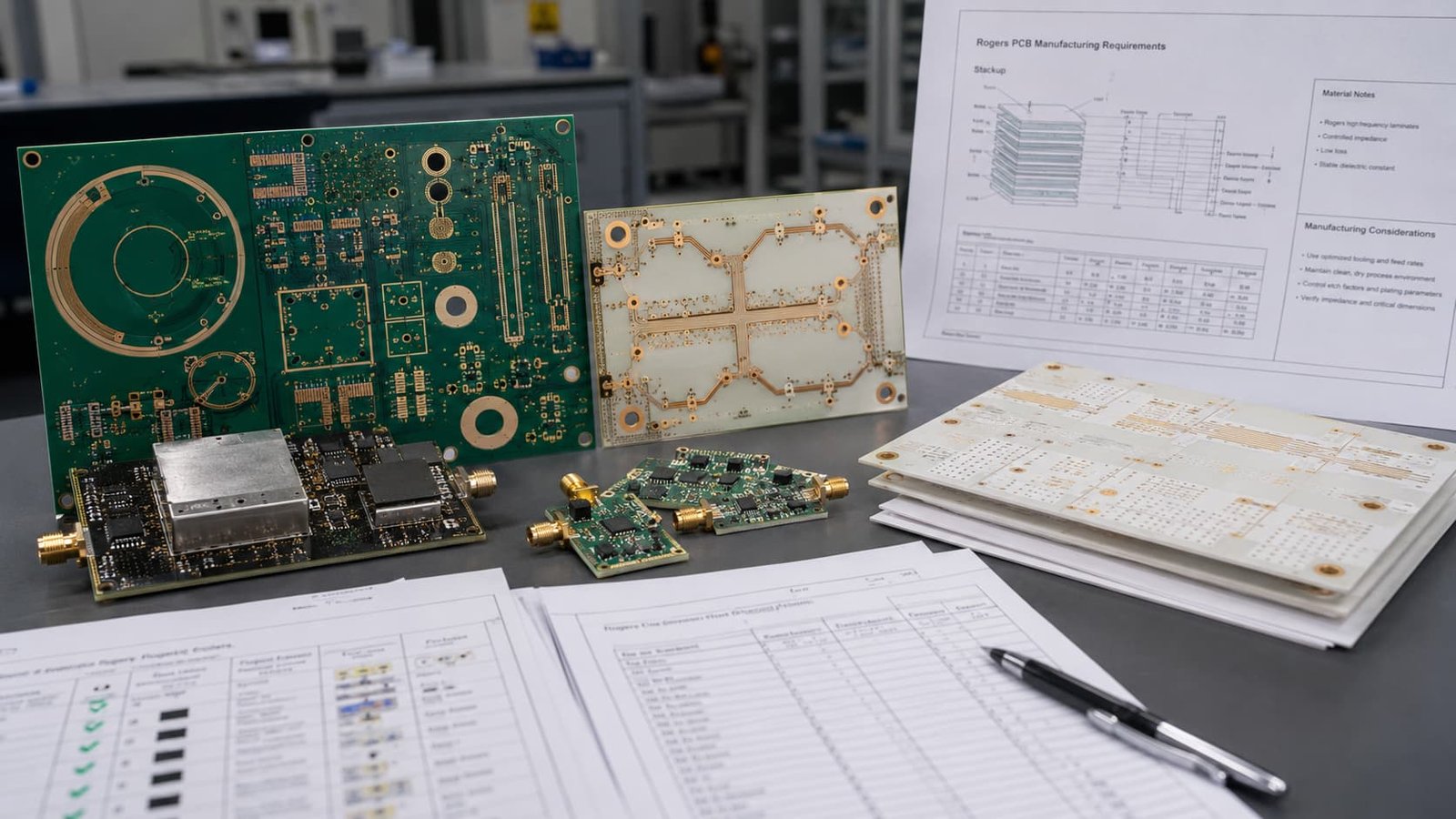
For buyers and engineers, Rogers PCB manufacturing should be reviewed before production starts. Key points include stackup design, material selection, drilling quality, plated through-hole reliability, copper thickness, controlled impedance, surface finish, and final inspection.
Quick Summary
Rogers PCB manufacturing is commonly used for RF, microwave, antenna, radar, satellite communication, wireless infrastructure, and high frequency signal applications.
The most important manufacturing requirements include accurate stackup design, stable dielectric thickness, controlled impedance, proper drilling, reliable plated through holes, suitable surface finish, and engineering review before production.
Rogers PCB projects may use single-sided, double-sided, multilayer, or FR4 + Rogers hybrid stackups depending on the application.
For RF and microwave performance, small changes in material thickness, copper thickness, trace geometry, or surface finish may affect the final result.
Riching PCB supports Rogers PCB manufacturing, Rogers materials, PTFE PCB manufacturing, and RF PCB manufacturing for high frequency PCB projects. Riching PCB’s Rogers Materials page also lists RO4000 series, RT/duroid series, high frequency RF laminates, microwave PCB materials, and Rogers + FR4 hybrid stackups as supported directions.
Why Rogers PCB Manufacturing Needs Engineering Review
Rogers PCB materials are selected when the circuit requires stable high frequency performance. Compared with general FR4 boards, RF and microwave circuits are more sensitive to material behavior and manufacturing tolerance.
If the stackup, drill quality, copper thickness, or surface finish is not controlled properly, the finished board may still pass visual inspection but fail RF testing.
Common risks include:
Impedance deviation
Higher signal loss
Poor plated through-hole reliability
Dimensional variation
Unstable RF performance
Surface finish mismatch
Stackup inconsistency
Production repeatability problems
For this reason, Rogers PCB projects should go through engineering review before quotation and before manufacturing.
Rogers PCB Stackup Requirements
The stackup is one of the most important parts of Rogers PCB manufacturing.
A Rogers PCB stackup should clearly define:
Material type
Layer count
Dielectric thickness
Copper thickness
Signal layers
Ground planes
Power layers
Final board thickness
Controlled impedance requirement
Hybrid material structure if used
For RF PCB and microwave PCB projects, the stackup is part of the electrical design. It should not be changed casually during production.
If the dielectric thickness changes, the impedance may change. If the copper thickness changes, the trace width and final RF behavior may also change. If the material is substituted without approval, the signal loss and Dk behavior may no longer match the original design.
For related stackup planning, you can also connect this topic with RF PCB Stackup Design and FR4 + Rogers Hybrid PCB Stackup.
Single-Sided and Double-Sided Rogers PCB
Some Rogers PCB projects are simple single-sided or double-sided boards. These may be used for RF modules, antenna boards, filters, test circuits, or signal transmission boards.
Even simple Rogers PCB structures still require careful review of material thickness, copper thickness, trace accuracy, and surface finish.
For double-sided Rogers PCB, plated through holes and via connections may also become important. The manufacturer should confirm whether the holes are used for signal transitions, grounding, connectors, or mechanical functions.
Multilayer Rogers PCB
Multilayer Rogers PCB is used when the design requires RF layers, ground planes, power layers, control circuits, or mixed signal structures in one board.
Multilayer Rogers PCB manufacturing requires more process control because lamination, registration, drilling, and plated through holes become more complex.
Important points include:
Layer alignment
Lamination control
Material compatibility
Dielectric thickness control
Copper balance
Ground reference continuity
Controlled impedance calculation
Final board thickness tolerance
For high frequency multilayer PCB, the manufacturer should review whether the proposed structure is practical for both electrical performance and production reliability.
FR4 + Rogers Hybrid Stackup
Some projects use Rogers material only on RF layers and FR4 on non-RF layers. This is called an FR4 + Rogers hybrid stackup.
Hybrid stackups can help balance RF performance and cost, especially when only part of the board carries high frequency signals.
However, hybrid PCB manufacturing requires careful review because Rogers materials and FR4 may have different thermal, mechanical, and lamination behavior. Rogers’ RO4000 processing guideline notes that RO4003C, RO4350B, and RO4835 laminates can be processed through standard acid copper and electrolytic tin or tin/lead plating processes, and do not require special treatments before metallization.
Before production, the manufacturer should review:
Material compatibility
Prepreg or bonding system
Layer symmetry
Warpage risk
Drilling behavior
Plated through-hole reliability
Lamination process
Controlled impedance target
A hybrid stackup can be useful, but it should not be treated as a simple material combination.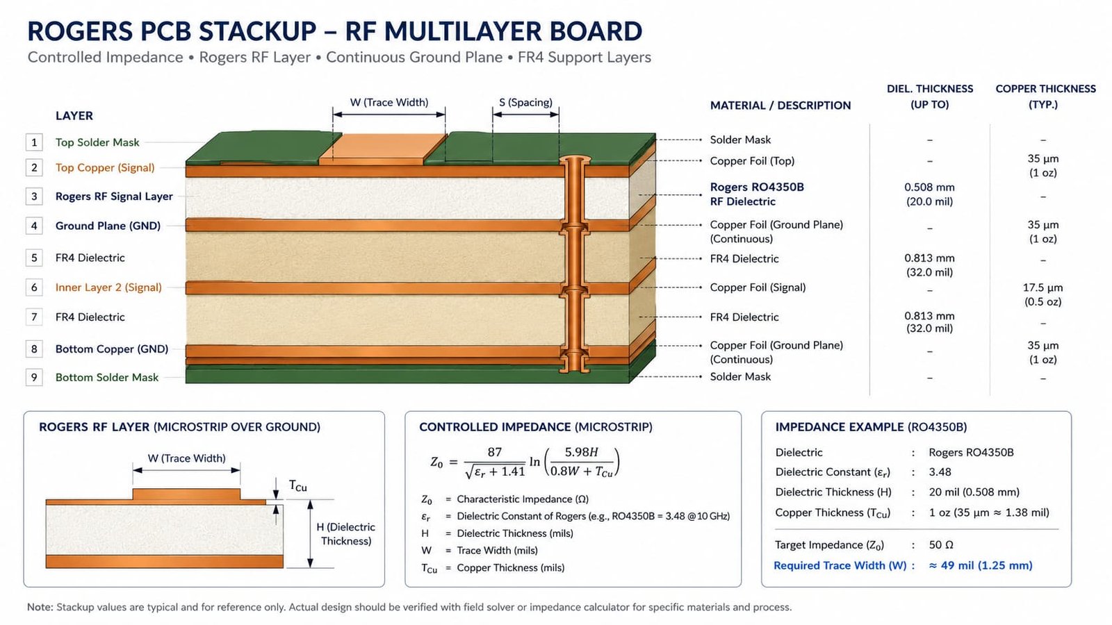
Drilling Requirements for Rogers PCB
Drilling is a critical step in Rogers PCB manufacturing.
Poor drilling can cause hole roughness, resin smear, poor plating adhesion, dimensional issues, or reliability problems. For RF and microwave PCB projects, drilling quality may also affect grounding vias, RF transitions, connector holes, and plated through-hole performance.
Important drilling considerations include:
Drill size
Hole tolerance
Material type
Board thickness
Copper thickness
Hole density
Via structure
Connector hole requirement
Plated or non-plated holes
If the board uses small vias, dense ground vias, RF via transitions, or connector areas, drilling should be reviewed carefully before production.
For deeper related content, this topic can connect naturally with Via Design Considerations for RF PCB Manufacturing.
Plated Through-Hole Reliability
Plated through holes are important for multilayer Rogers PCB, hybrid PCB, and RF PCB structures.
In RF applications, plated through holes may be used for:
Ground connections
RF layer transitions
Connector grounding
Via fences
Thermal paths
Mechanical connection
Component mounting
The plating must be stable and reliable. Poor plated through-hole quality may cause electrical failure, weak grounding, intermittent connection, or long-term reliability issues.
For Rogers PCB and Rogers + FR4 hybrid stackups, plated through-hole reliability should be reviewed together with material behavior, lamination quality, drilling process, and copper plating control.
Controlled Impedance Manufacturing
Controlled impedance is often required in Rogers PCB projects.
Impedance depends on:
Material Dk
Dielectric thickness
Trace width
Copper thickness
Reference plane
Solder mask
Surface finish
Manufacturing tolerance
Before production, the manufacturer should confirm the impedance target and tolerance. If the customer provides an impedance table, the stackup should be reviewed to confirm whether the target values are achievable.
For RF and microwave applications, impedance should be reviewed before manufacturing, not after the board is finished. This section can be supported by your article Why Controlled Impedance Matters in RF PCB Manufacturing.
Copper Thickness and Etching Control
Copper thickness affects impedance, current capacity, etching accuracy, and RF performance.
For Rogers PCB manufacturing, both base copper and finished copper should be confirmed. If plated copper increases the finished thickness, the trace geometry may change.
Important copper-related points include:
Outer layer copper thickness
Inner layer copper thickness
Finished copper requirement
Etching tolerance
Trace width accuracy
RF trace geometry
Copper balance
For fine RF traces, the manufacturer should control etching carefully to maintain trace accuracy and impedance stability.
Surface Finish for Rogers PCB
Surface finish protects exposed copper and supports soldering or assembly.
Common surface finishes for Rogers PCB may include:
ENIG
Immersion silver
OSP
HASL
Lead-free HASL
Hard gold for contact areas
Customer-specified finishes
ENIG is commonly used for many Rogers PCB projects because it provides a flat surface and stable solderability. Immersion silver may be considered for some RF applications where conductivity and surface flatness are important. OSP may be used in some controlled assembly conditions, while HASL is usually reviewed carefully because surface flatness may be a concern.
Surface finish should be selected based on assembly method, RF sensitivity, storage requirement, connector area, bonding requirement, and customer specification.
For more detail, this section can connect with Surface Finish Options for RF and Microwave PCB.
Inspection and Quality Control
Rogers PCB projects should be inspected carefully before shipment.
Common inspection items include:
Visual inspection
Dimensional inspection
Hole quality inspection
Copper thickness check
Surface finish inspection
Electrical testing
Impedance testing if required
Final board thickness check
Material verification
Packaging review
For RF and microwave PCB projects, impedance testing may be required if the design includes controlled impedance traces. Test coupons may be used depending on customer requirements.
Information Needed Before Production
To manufacture Rogers PCB accurately, buyers should provide complete project information.
Recommended files and details include:
Gerber files
Drill files
PCB stackup
Rogers material requirement
Board thickness
Copper thickness
Surface finish
Controlled impedance requirement
Layer count
Quantity
Working frequency
Application background
Special reliability requirements
If the exact Rogers material is not confirmed, the manufacturer can review the design and suggest possible material options based on frequency, signal loss requirement, stackup, and production feasibility.
For preparation before quotation, you can also connect this article with What Files Are Needed for a High Frequency PCB Quotation?.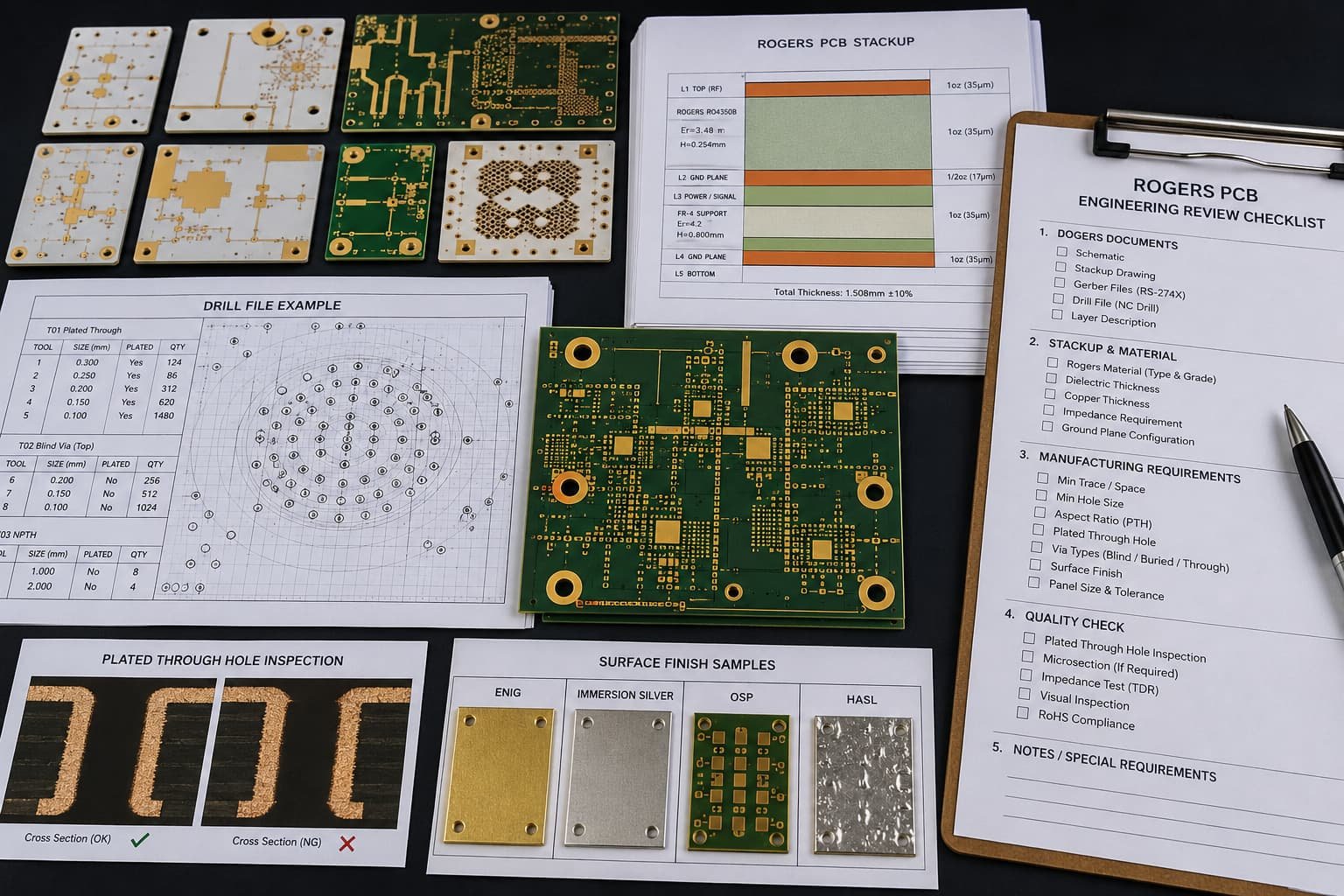
Conclusion
Rogers PCB manufacturing requires careful review of stackup, material selection, dielectric thickness, copper thickness, drilling, plated through-hole reliability, controlled impedance, surface finish, and final inspection.
For RF PCB, microwave PCB, antenna PCB, radar electronics, satellite communication, 5G devices, and high frequency communication boards, small manufacturing variations can affect final performance.
Before production, buyers should provide complete Gerber files, drill files, stackup, material requirement, copper thickness, surface finish, impedance details, quantity, and application background. Early engineering review can help reduce production risk and improve Rogers PCB manufacturing consistency.