Satellite communication PCB projects usually sit in the higher-risk side of RF and microwave manufacturing. The board is not only carrying components. In many designs, the material, stackup, RF traces, ground reference, vias, antenna feed lines, and surface finish all become part of the signal path.
For buyers, the main question is not just “Can this PCB factory produce the board?” A better question is: can the manufacturer review the RF requirement, material behavior, stackup, impedance, drilling, and production tolerance before the board goes into fabrication?
Satellite communication boards may use high frequency PCB, RF PCB, microwave PCB, antenna PCB, Rogers materials, PTFE laminates, Taconic materials, F4B materials, or hybrid stackups depending on frequency, signal loss, size, reliability target, and cost.
Rogers describes its RT/duroid laminates as filled PTFE composite materials for high reliability, aerospace, defense, RF, and microwave applications. For satellite communication PCB projects, this kind of material information is useful when reviewing low-loss RF and microwave requirements.
Quick Summary
Satellite communication PCB projects often require low-loss materials, controlled impedance, stable stackup design, reliable vias, and careful RF layout review.
Common PCB types include RF PCB, microwave PCB, antenna PCB, phased-array antenna boards, RF front-end boards, and signal processing boards.
Material choice should be reviewed by working frequency, Dk, Df, board thickness, copper thickness, controlled impedance target, and application environment.
Before quotation, buyers should prepare Gerber files, drill files, PCB stackup, material requirement, controlled impedance information, quantity, working frequency, and application background.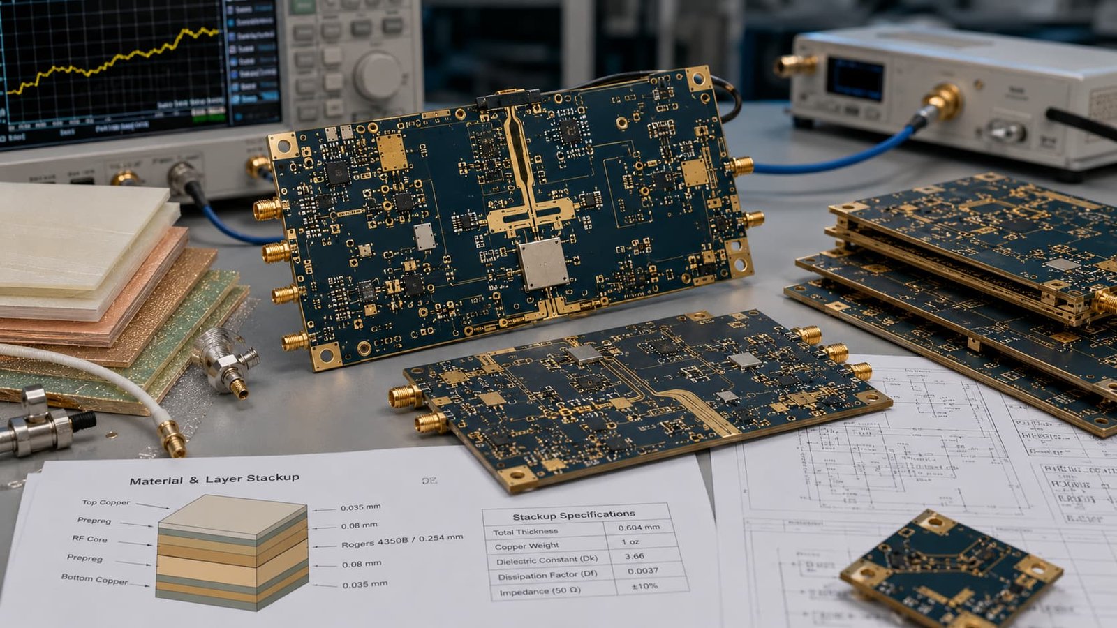
Where Satellite Communication PCBs Are Used
Satellite communication products may include several different PCB types inside one system. Some boards handle RF transmission, some support antenna networks, and others connect control, power, or signal processing sections.
Common applications include:
Satellite antenna systems
RF front-end modules
Microwave communication circuits
Antenna feed networks
Power amplifier boards
Low-noise amplifier circuits
Filters and signal paths
Ground station communication equipment
High frequency test boards
Aerospace RF modules
A low-speed control section may not need high frequency material. But the RF signal layer, antenna feed network, or microwave path usually needs a much more careful material and stackup review.
For antenna-related designs, Antenna PCB for Wireless Devices and RF Front-End Modules follows the same logic: the antenna area, feed line, ground plane, and material cannot be reviewed separately.
Material Selection Is the First Risk Point
In satellite communication PCB projects, material choice usually drives the rest of the manufacturing review.
A material should be selected around the real signal requirement, not only around a familiar brand name. The review should include:
Working frequency
Dk and Df values
Dk tolerance
Dielectric thickness
Copper type
Copper thickness
Signal loss target
Controlled impedance requirement
Thermal and mechanical behavior
Availability for prototype and batch production
Rogers’ official RO4000 Series Laminates page is often used as a reference for low-loss high frequency materials used in RF, microwave, and millimeter-wave applications. For more demanding PTFE-based options, RT/duroid PCB materials may also be reviewed.
Riching PCB also supports Rogers materials, PTFE PCB manufacturing, Taconic materials, and F4B materials for different RF and microwave PCB requirements.
Dk and Df Should Not Be Treated as Simple Numbers
For satellite communication PCB, Dk and Df directly affect the design result.
Dk affects impedance, wavelength, phase behavior, antenna dimensions, and trace geometry. Df affects dielectric loss and insertion loss. If the material is selected only by price or availability, the final board may not meet the expected RF behavior.
This is why the material should be reviewed together with the stackup. A low-loss laminate may still create problems if the dielectric thickness, copper thickness, or trace width does not match the impedance target.
Rogers’ technical article on dielectric constant in PCB materials is useful for understanding why Dk depends on more than one simple datasheet number. Riching PCB’s article How Dk and Df Affect High Frequency PCB Performance explains the same issue from a manufacturing and quotation review perspective.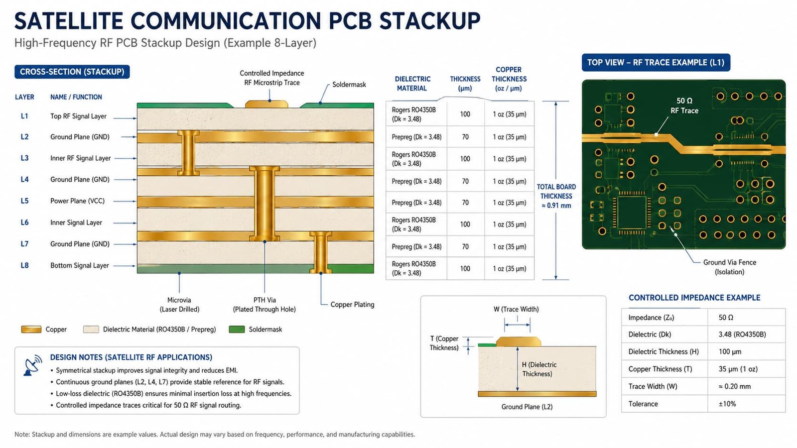
Stackup Review Before Production
The stackup should be confirmed before the manufacturer starts production. In satellite communication PCB projects, the stackup is part of the RF design.
A useful stackup review should include:
Layer count
Material type
Dielectric thickness
Copper thickness
RF signal layers
Ground reference planes
Power layers
Final board thickness
Controlled impedance target
Via structure
Surface finish
Hybrid material structure if used
If the dielectric thickness changes, impedance may change. If copper thickness changes, trace width and loss behavior may shift. If the reference ground plane is not continuous, the RF return path may become unstable.
Controlled Impedance Cannot Be an Afterthought
Satellite communication PCB designs often include RF traces, microwave paths, antenna feed lines, filters, connector launches, and phased-array structures. Many of these features need controlled impedance.
A manufacturer should review:
Target impedance
Tolerance requirement
Trace structure
Layer location
Reference plane
Material Dk
Dielectric thickness
Copper thickness
Solder mask condition
Impedance test requirement
If impedance is not defined before production, the board may be fabricated correctly from a mechanical view but still fail RF testing.
For a deeper explanation, Riching PCB’s controlled impedance RF PCB article covers why impedance control must be planned before manufacturing, not corrected after the board is finished.
RF Layout and Grounding Review
RF layout review is one of the most practical ways to reduce prototype risk.
The review should check RF traces, bends, transitions, component pads, connectors, ground vias, antenna keep-out areas, and return paths. Analog Devices’ RF and mixed-signal PCB layout guidance is a useful reference for RF board layout discipline, especially around transmission lines, grounding, and separation of sensitive signals.
Satellite communication PCB layout review should check:
RF trace width and spacing
Ground plane continuity
Connector launch areas
Antenna feed lines
Via transitions
Ground via placement
Copper clearance
Shielding areas
Signal isolation
Surface finish requirement
A good material cannot compensate for a broken ground reference or poor transition structure. This is why RF PCB layout review before manufacturing should be part of the production preparation process.
Vias and Plated Through Holes
Vias are easy to underestimate in satellite communication PCB projects.
A via can be a signal transition, ground connection, thermal path, shielding feature, or part of a via fence. At microwave frequencies, via geometry may affect performance more than expected.
The review should include:
Signal via size
Ground via spacing
Via stub length
Anti-pad design
Plated through-hole reliability
Via fence placement
Connector grounding
Layer transition path
For multilayer boards or hybrid stackups, plated through-hole reliability should be reviewed carefully. This is especially true when the board uses PTFE, Rogers, Taconic, or mixed material systems.
Surface Finish and Assembly Review
Surface finish should be selected around the assembly process and RF requirement.
Common surface finishes include:
ENIG
Immersion silver
OSP
HASL
Lead-free HASL
Hard gold for contact areas
Customer-specified finishes
ENIG is commonly used in many RF and microwave PCB projects because it provides a flat surface and stable solderability. Immersion silver may be considered for certain RF-sensitive applications. HASL should be reviewed carefully if flatness is important.
For satellite communication PCB, finish selection should consider solderability, storage, connector areas, bonding requirements, RF pad behavior, and customer specification.
Riching PCB’s Surface Finish Options for RF and Microwave PCB explains how finish selection affects high frequency PCB manufacturing and assembly review.
What Buyers Should Prepare for Quotation
A satellite communication PCB quotation should not be based only on Gerber files.
Buyers should prepare:
Gerber files
Drill files
Full PCB stackup
Material requirement
Board thickness
Copper thickness
Surface finish
Controlled impedance requirement
Working frequency
Layer count
Quantity
Prototype or batch requirement
Application background
Special reliability requirements
If the exact material is not confirmed, the working frequency and application background are very useful. A manufacturer can only provide meaningful material advice when the RF requirement is clear.
Riching PCB’s high frequency PCB quotation files checklist can help buyers prepare cleaner files before sending the project for review.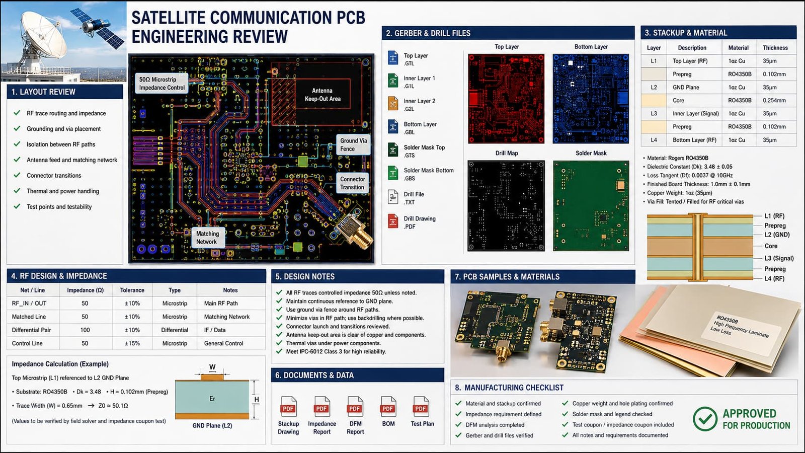
Common Mistakes to Avoid
The most common mistake is treating a satellite communication PCB like a normal multilayer board.
Other common problems include:
Material selected only by cost
No working frequency provided
Missing impedance table
Unclear stackup
Ground plane breaks under RF traces
Poor connector transition
Via stubs ignored
Surface finish chosen by habit
No review of material availability
Prototype and batch requirements not discussed
These issues often appear during testing, not during visual inspection. A board can look clean and still fail RF performance requirements.
Conclusion
Satellite communication PCB projects need more than standard PCB fabrication. Material selection, Dk and Df, stackup, controlled impedance, RF layout, vias, plated through holes, surface finish, and quotation details all affect the final result.
For RF modules, microwave communication circuits, antenna systems, satellite ground equipment, and high frequency signal boards, the safest path is to review the design before production begins.
A strong PCB manufacturer should not only quote the board. It should also help review whether the material, stackup, impedance, and manufacturing process match the satellite communication requirement.