RF PCB impedance testing fails when the finished board does not match the impedance target defined in the design or stackup. The reason is usually not one single mistake. It may come from material changes, dielectric thickness variation, copper thickness, trace width tolerance, solder mask, via transitions, or a stackup that was not confirmed before production.
For RF and microwave boards, impedance is not just a drawing requirement. It is the result of material, geometry, copper, reference plane, and manufacturing control working together. If one of these items changes, the impedance result can shift.
For buyers, an impedance failure usually means more than a test report problem. It may cause signal reflection, unstable RF performance, redesign delays, or a second prototype run.
Quick Summary
RF PCB impedance testing may fail because of stackup mismatch, wrong dielectric thickness, trace width deviation, copper thickness variation, material substitution, poor etching control, solder mask effect, or incorrect impedance coupon design.
Controlled impedance should be reviewed before fabrication, not after the board is finished.
A complete quotation request should include Gerber files, drill files, stackup, impedance table, material requirement, copper thickness, board thickness, surface finish, and working frequency.
For RF PCB projects, the manufacturer should confirm whether the production stackup can meet the requested impedance target before starting fabrication.
1. Stackup Was Not Confirmed Before Production
One of the most common reasons for impedance failure is a stackup mismatch.
The designer may calculate impedance using one dielectric thickness, but the manufacturer may build the board using another available core or prepreg thickness. Even if the change looks small mechanically, it can affect impedance.
Important stackup details include:
Material type
Dielectric thickness
Copper thickness
Layer count
RF signal layer
Ground reference plane
Final board thickness
Solder mask condition
Impedance tolerance
In RF PCB manufacturing, stackup should be confirmed before production. If the factory changes material thickness without recalculating impedance, the finished board may fail the test even when the Gerber data looks correct.
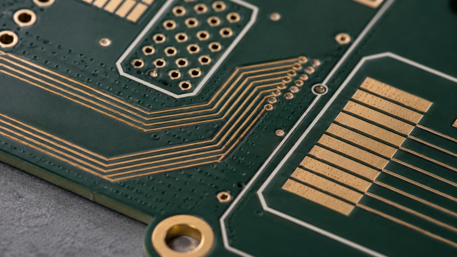
2. Trace Width Changed During Etching
Controlled impedance traces depend heavily on final trace width.
During fabrication, copper etching can make traces slightly narrower or wider than the design value. This may happen because of copper thickness, etching compensation, line spacing, panel position, or process control.
For standard PCB, a small trace width change may not matter much. For RF PCB, especially narrow impedance traces, it may shift the result enough to fail testing.
Buyers should avoid sending only Gerber files without impedance requirements. The manufacturer needs to know which traces are impedance controlled and what tolerance is required.
3. Copper Thickness Was Different From the Design
Copper thickness affects impedance and loss.
If the design assumes 1 oz copper but the production stackup uses another thickness, the impedance calculation may no longer be valid. Plating can also affect the final copper thickness, especially in multilayer boards or designs with plated through holes.
Copper thickness should be confirmed for:
Outer layers
Inner layers
Finished copper thickness
Plated hole requirement
RF trace layer
Power or thermal copper areas
For RF boards, copper thickness should not be treated only as a current-carrying parameter. It also affects trace geometry, impedance, and manufacturing tolerance.
4. Material Was Substituted
Material substitution is another common risk.
A buyer may request one high frequency laminate, but a similar-looking material may be suggested because of cost, lead time, or availability. This can be acceptable only when the RF requirement is reviewed carefully.
Material changes can affect:
Dk value
Df value
Dk tolerance
Dielectric thickness
Thermal behavior
Copper type
Manufacturing process
Batch consistency
For impedance testing, Dk and dielectric thickness are especially important. A material substitution should never be treated as a simple purchasing decision. Engineering review is needed before approval.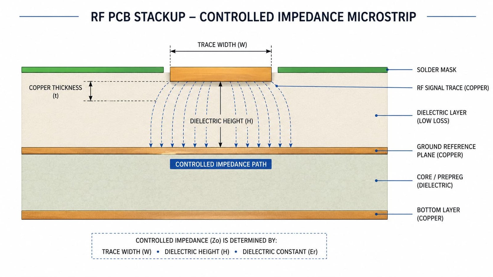
5. Solder Mask Was Not Considered
Solder mask can affect impedance when it covers RF traces.
Some RF designs calculate impedance with solder mask included. Others assume exposed copper or no solder mask over the RF path. If the production condition does not match the calculation, the impedance result may change.
This is especially relevant for microstrip structures on outer layers.
Before production, the buyer and manufacturer should confirm:
Whether RF traces are covered by solder mask
Solder mask thickness assumption
Exposed RF copper requirement
Surface finish requirement
Impedance calculation condition
A small mismatch here can cause confusion during testing because the board may be manufactured correctly, but not according to the intended impedance model.
6. Reference Plane Was Broken or Too Far Away
Controlled impedance needs a stable reference plane.
If the RF trace does not have a continuous ground plane under it, the return path becomes unstable. This can affect impedance, signal quality, and RF performance.
Common issues include:
Ground plane cutout under RF trace
Split plane crossing
Poor via stitching
Large clearance near RF path
Wrong layer reference
Unexpected copper removal
This kind of issue may not always be caught by basic DFM checks. RF layout review is needed, especially around connectors, layer transitions, filters, and antenna feed lines.
7. Via Transitions Created Discontinuity
Vias can also affect impedance.
In high frequency RF systems, vias may be used for signal transitions, ground stitching, shielding, and connector grounding. If the via transition is not designed well, it may create reflection or impedance discontinuity.
Important via points include:
Signal via size
Pad size
Anti-pad clearance
Via stub length
Ground via spacing
Reference plane connection
Layer transition path
For higher-frequency boards, via stubs and poor grounding can become more visible in testing. Via review should happen during layout and manufacturing preparation, not after the board fails.
8. Impedance Coupon Did Not Match the Real Trace
Impedance is often tested using coupons placed on the production panel. If the coupon does not match the real controlled impedance trace structure, the test report may not represent the actual circuit.
A coupon should match:
Layer structure
Trace width
Trace spacing
Copper thickness
Dielectric thickness
Reference plane
Solder mask condition
Impedance type
If the coupon is designed incorrectly, the test report may pass while the actual RF path is not correct, or the coupon may fail while the real circuit performs differently.
9. Production Variation Between Prototype and Batch
Another problem appears when the prototype passes, but the batch fails.
This may happen because of material lot changes, stackup adjustment, panel layout change, copper thickness variation, different surface finish, or changed production process.
For RF PCB projects evaluated through standard IPC design rules, buyers should confirm whether the approved prototype stackup can be repeated in batch production. If the design is sensitive, the same material family, dielectric thickness, copper specification, and impedance testing method should be maintained.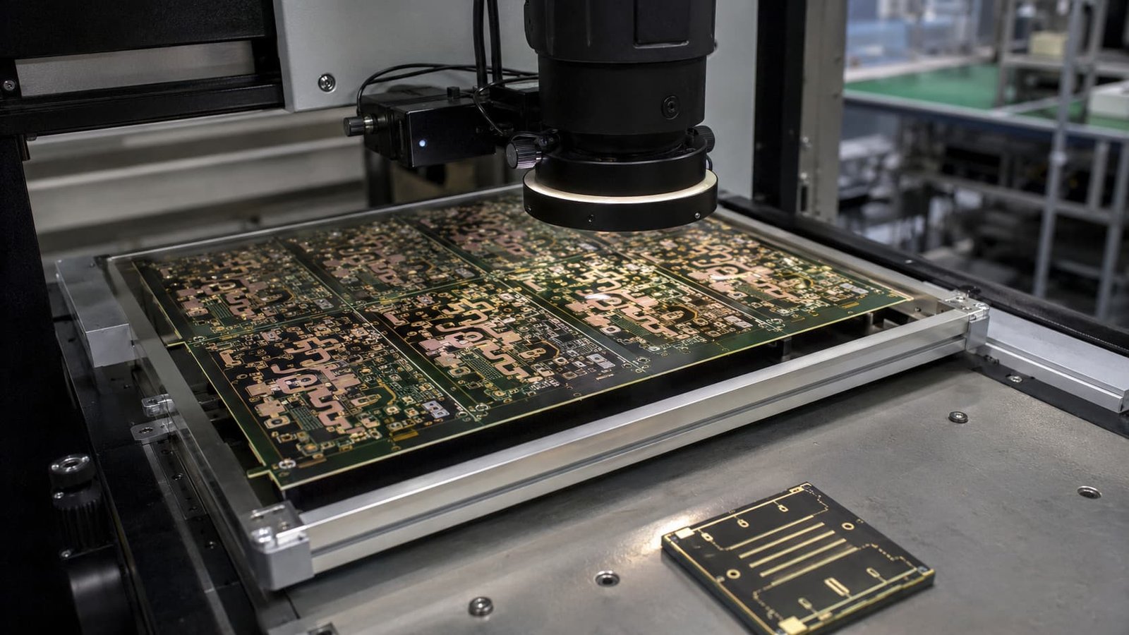
What Buyers Should Provide Before Quotation
To reduce impedance failure risk, buyers should prepare:
Gerber files
Drill files
PCB stackup
Material requirement
Controlled impedance table
Target impedance and tolerance
Board thickness
Copper thickness
Surface finish
Solder mask requirement
Working frequency
Quantity
Prototype or batch plan
Application background
If the stackup is not fixed, the manufacturer should help review a practical production stackup before confirming the quotation.
Common Mistakes to Avoid
Common mistakes include:
Sending Gerber files without stackup
No impedance table
Changing material after layout
Ignoring solder mask effect
Assuming all RF traces are the same
Not defining impedance tolerance
No impedance coupon requirement
Changing copper thickness during production
Ignoring reference plane breaks
Not discussing batch repeatability
Most of these problems can be reduced before fabrication if the quotation request is complete and the manufacturer reviews the RF requirement carefully.
Conclusion
RF PCB impedance testing fails when design assumptions and manufacturing reality do not match. Stackup, material, dielectric thickness, copper thickness, trace width, solder mask, reference plane, vias, and test coupons all affect the final result.
For buyers, the best way to reduce impedance risk is to provide complete manufacturing information before production. Gerber files alone are not enough for serious RF PCB projects.
A good RF PCB manufacturer should review the stackup, material, impedance target, trace structure, copper thickness, vias, and testing method before fabrication starts. That review is often the difference between a board that only looks correct and a board that performs correctly.