Ka-Band PCB: Materials, Design Rules and Manufacturing Guide

Material selection, stackup design and process requirements for Ka-band PCB operating from 26.5 GHz to 40 GHz — satellite communication, 5G mmWave and defense applications.

Table of Contents

Key point: Most factories quote 3–4 weeks waiting for RO3003 / RT5880 material procurement. Riching PCB maintains these materials in stock — no material wait.Ka-band PCB (26.5–40 GHz) requires PTFE substrate — Rogers RO3003 (Dk 3.0, Df 0.0010) or RT5880 (Dk 2.20, Df 0.0009). Rogers RO4350B (Df 0.0037) produces unacceptable insertion loss at Ka-band. All PTFE materials require in-house plasma hole wall activation before copper plating, low-profile copper foil, ENIG surface finish, and TDR impedance verification to ±5% on every production lot. Maximum 2 lamination press cycles for PTFE. Riching PCB stocks RO3003 and RT5880 with in-house plasma activation. No MOQ. Prototype lead time 7–10 working days.

Ka-band PCB operates from 26.5 GHz to 40 GHz — a frequency range where standard FR4 is completely unusable and even Rogers RO4350B produces unacceptable insertion loss for most applications. At Ka-band, the signal wavelength in the substrate is 3–5 mm. Dielectric loss, copper surface roughness, and Dk variation over temperature all become first-order design constraints rather than secondary concerns.

This guide covers Ka-band frequency sub-bands and applications, material selection, design rules, manufacturing requirements, and what to verify with your fabricator before placing an order.

Ka-Band Frequency Range and ApplicationsKa-band frequency range diagram showing satellite uplink and downlink bands 26.5 to 40 GHz

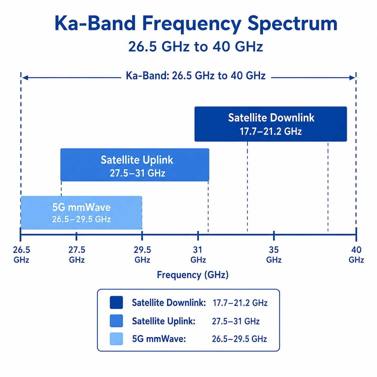
Ka-band covers 26.5–40 GHz and is divided into several sub-bands with distinct applications:

  • Satellite communication uplink: 27.5–31 GHz — VSAT terminals, HTS (High Throughput Satellite) ground terminals, LEO constellation user terminals (Starlink, OneWeb)
  • Satellite communication downlink: 17.7–21.2 GHz (upper Ku/lower Ka overlap)
  • 5G mmWave: 26.5–29.5 GHz — 5G NR FR2 base station and CPE antenna PCB
  • Defense and radar: 33–36 GHz — airborne weather radar, missile seeker, fire control radar
  • Point-to-point backhaul: 27.5–40 GHz — microwave backhaul links
  • Scientific: 31.8–33 GHz — radio astronomy, atmospheric research

Why Ka-Band Requires PTFE Substrate

At 26.5–40 GHz, dielectric loss dominates insertion loss. Rogers RO4350B (Df 0.0037) — the standard material for RF applications below 12 GHz — produces insertion loss of approximately 3–5 dB/cm at Ka-band. Over a 5 cm trace, this represents 15–25 dB of loss before the signal reaches the antenna — far beyond any practical link budget.

PTFE substrates (RO3003, RT5880) with Df of 0.0009–0.0010 reduce insertion loss to approximately 0.5–1 dB/cm at Ka-band, preserving signal integrity across the board. Dk stability is equally critical: at 30 GHz, a ±0.05 variation in Dk shifts a patch antenna resonance by approximately 500 MHz — pushing the antenna out of band.

Material Selection for Ka-Band PCB

Material Dk Df Type Notes for Ka-band
RO3003 3.0 0.0010 PTFE ceramic ✅ Most common — stable Dk, 0.127 mm standard thickness
RT5880 2.20 0.0009 PTFE glass ✅ Lowest loss — larger antenna element due to lower Dk
Taconic TLY-5 2.17 0.0009 PTFE glass ✅ Alternative to RT5880 — similar performance
F4BM220 2.20 0.0010 PTFE ✅ Cost-effective — confirm Dk stability at Ka-band
RO4350B 3.48 0.0037 Hydrocarbon ❌ Not recommended — Df too high for Ka-band

Rogers RO3003 (Dk 3.0, Df 0.0010) — Recommended

RO3003 is the most widely used material for Ka-band PCB. Its Dk of 3.0 provides good trace width (wider than RT5880, easier to manufacture) while its Df of 0.0010 keeps insertion loss within acceptable limits across the Ka-band. Available in 0.127 mm and 0.254 mm standard dielectric thickness. 0.127 mm is standard for most Ka-band patch antenna designs.

Rogers RT5880 (Dk 2.20, Df 0.0009) — Lower Loss

RT5880 offers the lowest Df of any standard Rogers material (0.0009) and is used where maximum range or minimum insertion loss is required. Lower Dk means wider traces for the same impedance but larger antenna element size. Both RO3003 and RT5880 are available in multiple thicknesses from Riching PCB.

Taconic TLY-5 and F4BM220 — Cost-Effective Alternatives

Taconic TLY-5 (Dk 2.17, Df 0.0009) and F4BM220 (Dk 2.20, Df 0.0010) offer similar electrical performance to RT5880 at lower material cost. Both are PTFE-based and require plasma hole wall activation. Confirm Dk stability at Ka-band operating temperature range with the material supplier before use in production designs.

Ka-Band PCB Design Rules

Parameter Typical Value Notes
Frequency range 26.5–40 GHz (Ka-band) Satellite: 27.5–31 GHz uplink, 17.7–21.2 GHz downlink
Substrate RO3003 or RT5880 PTFE required — plasma activation mandatory
Dielectric thickness 0.127–0.254 mm 0.127 mm most common for Ka-band antenna
Trace width (50Ω) ~0.28 mm on 0.127 mm RO3003 Confirm with fabricator TDR
Impedance tolerance ±5% or better TDR verification on every lot
Copper foil Low-profile or reverse-treated Standard ED copper increases loss at Ka-band
Surface finish ENIG HASL not acceptable — surface flatness critical
Min. line width 2.5 mil Verify with fabricator for PTFE process
Board thickness 0.2–0.8 mm typical Thin substrate required for Ka-band antenna arrays
PTFE lamination limit Max 2 press cycles Exceeding causes Dk variation across board

Manufacturing Requirements

PTFE Plasma Activation

All Ka-band PCB substrates (RO3003, RT5880, Taconic, F4B) are PTFE-based and require plasma or sodium naphthalene hole wall activation before copper plating. Without this step, copper deposits on the PTFE hole wall with no mechanical adhesion — the board passes initial electrical testing and fails under thermal cycling. See PTFE PCB manufacturing requirements for full process detail. Riching PCB performs in-house plasma activation on every PTFE order as standard process.

Impedance Control

Ka-band PCB requires impedance tolerance of ±5% or better. Standard ±10% tolerance causes antenna resonance shift and pattern degradation at millimeter-wave frequencies. TDR verification must be performed on every production lot. Trace width must be calculated using confirmed production Dk from the material certificate — not nominal datasheet values.

Copper Foil

At Ka-band frequencies, skin depth is approximately 0.3 µm. Standard electrodeposited (ED) copper foil has surface roughness of 1–2 µm RMS, which significantly increases the effective signal path length and insertion loss. Low-profile (LP) or reverse-treated (RTF) copper foil with roughness below 0.5 µm RMS is required for Ka-band designs.

Surface Finish

ENIG (immersion gold) is the standard surface finish for Ka-band PCB. The flat, consistent surface is critical for microstrip trace impedance uniformity. HASL produces surface topology variation of 5–15 µm — unacceptable at Ka-band. Immersion silver is acceptable for prototype evaluation.

PTFE Lamination Limit

PTFE materials are limited to a maximum of 2 lamination press cycles. For multi-layer Ka-band designs requiring Rogers + FR4 hybrid stackups, consult your fabricator on bondply selection and press cycle constraints before finalizing the stackup.

Rogers + FR4 Hybrid Stackup for Ka-Band

For multi-layer Ka-band designs where cost reduction is a priority, Rogers RO3003 + FR4 hybrid stackups place the PTFE material only on the outer RF signal layers while using FR4 for internal power and ground planes. This significantly reduces material cost compared to an all-PTFE board. See FR4 + Rogers hybrid PCB stackup guide for detailed design rules and bondply selection.

ApplicationsKa-band satellite communication PCB with patch antenna array on Rogers PTFE substrate

  • VSAT and HTS satellite terminal antenna PCB — Ku/Ka-band ground terminals
  • LEO constellation user terminal PCB — Starlink, OneWeb, Amazon Kuiper CPE
  • 5G NR FR2 base station antenna PCB — 26.5–29.5 GHz mmWave
  • Defense radar — airborne fire control, missile seeker, SAR radar
  • Point-to-point microwave backhaul — 27.5–40 GHz
  • Electronic warfare — Ka-band EW receiver and jammer PCB

Conclusion

Ka-band PCB (26.5–40 GHz) requires PTFE substrate — Rogers RO3003 or RT5880 — with in-house plasma activation, low-profile copper foil, ENIG surface finish, and TDR-verified impedance control to ±5%. RO4350B and standard FR4 are not suitable for Ka-band frequencies. Riching PCB manufactures Ka-band PCB with RO3003 and RT5880 in stock, in-house plasma activation, and prototype lead time of 7–10 working days. See high frequency PCB capabilities for full factory specifications.

Get a Quote for Your Ka-Band PCB

Riching PCB stocks RO3003 and RT5880 with in-house plasma activation. Send the following for DFM review:

  • Gerber files + NC drill file
  • Material grade (RO3003 or RT5880) and dielectric thickness
  • Stackup drawing — copper weight per layer
  • Controlled impedance target and tolerance
  • Operating frequency and application type
  • IPC Class and quantity

WhatsApp +86 13760473650 — DFM review within 24 hours

Q&A

Ka-Band PCB Q&A

Common questions about Ka-band PCB including material selection, why RO4350B is not suitable, impedance requirements, applications and prototype lead times.

What material is used for Ka-band PCB?

Rogers RO3003 (Dk 3.0, Df 0.0010) is the most common Ka-band material. RT5880 (Dk 2.20, Df 0.0009) offers lower loss. Taconic TLY-5 and F4BM220 are cost-effective PTFE alternatives. RO4350B (Df 0.0037) is not suitable — dissipation factor too high at Ka-band frequencies.

Why is RO4350B not suitable for Ka-band PCB?

RO4350B Df 0.0037 produces ~3–5 dB/cm insertion loss at Ka-band. Over 5 cm of trace, that is 15–25 dB of signal loss — far beyond any practical link budget. PTFE substrates (RO3003, RT5880) with Df 0.0009–0.0010 reduce insertion loss to ~0.5–1 dB/cm at Ka-band.

What impedance tolerance is required for Ka-band PCB?

±5% or better, verified by TDR on every production lot. At 30 GHz, ±10% impedance variation causes significant antenna pattern degradation and return loss. First article TDR alone is not sufficient — every production lot must be verified.

What are the main applications of Ka-band PCB?

VSAT and HTS satellite terminals, LEO constellation CPE (Starlink, OneWeb), 5G NR FR2 mmWave base station antenna PCB (26.5–29.5 GHz), defense radar (fire control, missile seeker), point-to-point microwave backhaul (27.5–40 GHz), and EW receiver/jammer PCB.

What is the lead time for Ka-band PCB prototype?

7–10 working days for RO3003 and RT5880 PTFE. No MOQ — from 1 board. DFM review before every order. WhatsApp: +86 13760473650.

PCB Project Review

Request a PCB Quote

Upload your Gerber ZIP file and project requirements. Our engineering team will review your PCB material, stackup, impedance needs, surface finish, and production quantity before quoting.

Please prepare:

  • Gerber files in ZIP format
  • PCB material or stackup requirements
  • Controlled impedance notes if available
  • Prototype or batch production quantity
ZIP format only. Please compress all Gerber and drill files into one ZIP package before uploading.