China PTFE PCB Manufacturer: How to Verify Real Plasma Activation Capability
7 questions that separate factories with genuine in-house plasma activation from those that outsource it, fake it, or don't know what you're asking about.
Home » China PTFE PCB manufacturer » China PTFE PCB Manufacturer: How to Verify Real Plasma Activation Capability
Table of Contents
Key point: Most Chinese PCB factories claiming PTFE capability do not have in-house plasma activation equipment. Plasma activation must be performed in-house, immediately before copper plating — outsourcing it produces boards that pass initial electrical testing and fail under thermal cycling. The fastest verification: ask for RO3003 prototype lead time. A factory with real PTFE capability answers 7–10 working days. A factory without it answers 5–7 days (same as FR4) — physically impossible if plasma activation is being performed correctly. Riching PCB performs in-house plasma activation on every PTFE order, RO3003 and RT5880 in stock, no MOQ.
China has hundreds of PCB factories claiming PTFE capability. Most of them are lying — or more precisely, most of them genuinely don’t understand why the claim is false. PTFE PCB requires in-house plasma hole wall activation before copper plating. A factory that outsources this step, skips it, or doesn’t have the equipment produces boards that pass all initial electrical tests and fail in the field under the first thermal cycle.
This guide gives you the exact questions to ask any Chinese PTFE PCB supplier, what correct answers look like, and what red flags tell you the factory doesn’t have the capability it claims.
Why Plasma Activation Is the Diagnostic Test
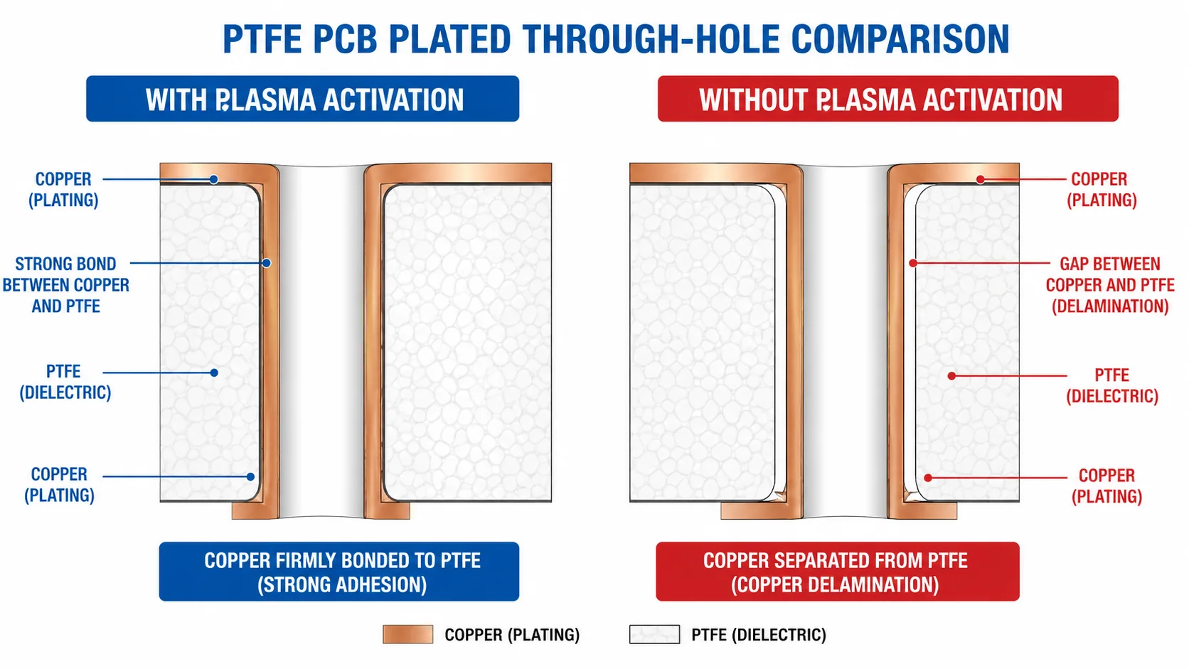
PTFE (polytetrafluoroethylene) is chemically inert. Copper cannot bond to it without surface treatment. Plasma activation or sodium naphthalene treatment etches the PTFE hole wall at the microscopic level, creating surface roughness that allows copper to mechanically anchor. Without it, electroplated copper sits on the PTFE surface with zero adhesion — it looks fine under visual inspection, passes continuity testing, and separates from the hole wall after 3–5 thermal cycles. See PTFE PCB manufacturing challenges for the full technical explanation.
This is why plasma activation is the single most important capability to verify. A factory with in-house plasma equipment has invested in real PTFE process capability. A factory without it — regardless of what its website says — cannot reliably manufacture Rogers RO3003, RT5880, Taconic TLY-5, F4B, or any other PTFE substrate.
The 3 Types of Chinese PCB Factories Claiming PTFE Capability

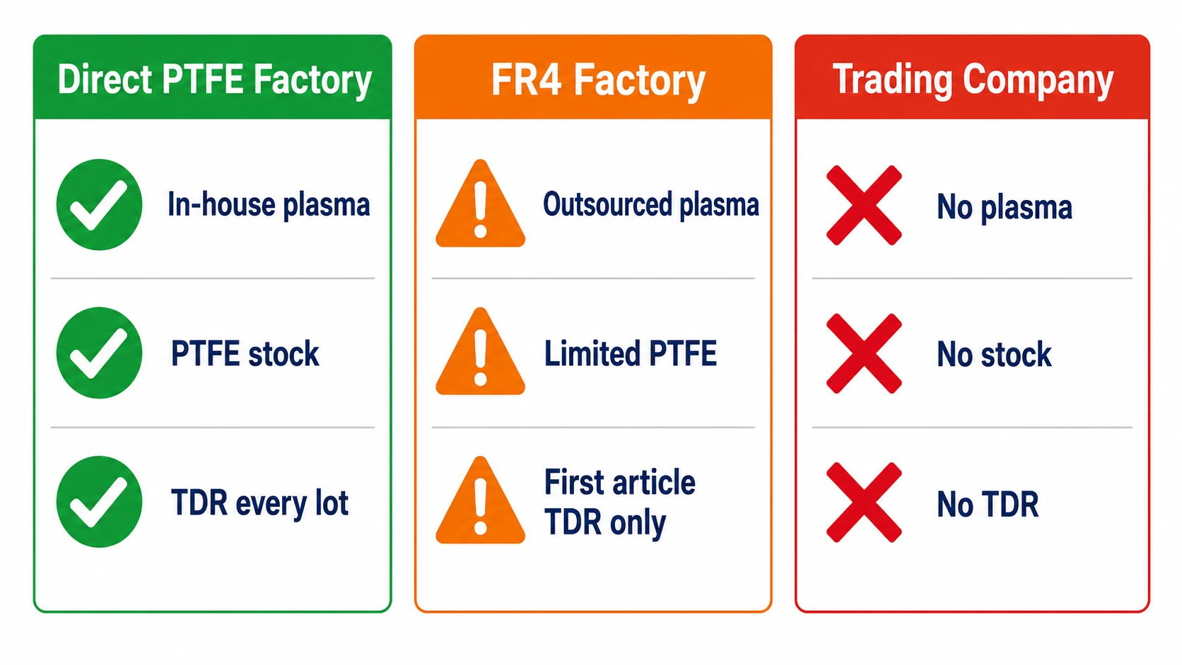
Type 1: Direct Factory with In-House Plasma (Rare — ~5% of suppliers)
These factories have plasma activation equipment on-site, operate it themselves, and perform activation on every PTFE order before copper plating. They have PTFE-specific drill programs, Rogers bondply in stock for hybrid stackups, and TDR verification capability. Lead time for RO3003 prototype is 7–10 working days because the PTFE process genuinely takes longer than FR4.
Type 2: FR4 Factory with Outsourced Plasma (Common — ~30% of suppliers)
These factories have FR4 capability and occasionally process PTFE orders by sending boards to a subcontractor for plasma activation. The process control gap is significant: plasma activation must be performed immediately before copper plating — any delay or environmental contamination between activation and plating reduces adhesion. Outsourced plasma means the factory cannot control this time window. Boards from these factories have inconsistent hole wall adhesion and higher field failure rates under thermal cycling.
Type 3: Trading Company or FR4-Only Factory (Majority — ~65% of suppliers)
These are either trading companies with no manufacturing capability, or FR4 factories that process PTFE substrates using FR4 parameters — no plasma activation, standard drill speed, standard press cycle. Boards from these factories fail predictably. The factories either don’t understand why, or they’re betting on the customer not testing thoroughly enough to catch it before the warranty period ends.
7 Questions to Ask Any Chinese PTFE PCB Supplier
| Question to Ask | Capable Factory Answer | Red Flag Answer |
|---|---|---|
| Is plasma activation in-house or outsourced? | ✅ In-house, our own equipment, every PTFE order | 🚩 We send it out / partner does it |
| How long after plasma before plating starts? | ✅ Within 2–4 hours, same day | 🚩 No specific answer given |
| Which Rogers PTFE grades do you stock? | ✅ RO3003, RT5880, RT5870 in stock | 🚩 We can source any Rogers material |
| Lead time for RO3003 prototype? | ✅ 7–10 working days | 🚩 5–7 days / same as FR4 |
| Drill parameters for PTFE? | ✅ Reduced spindle speed, PTFE-specific per grade | 🚩 Same as FR4 / standard parameters |
| Max lamination cycles for PTFE? | ✅ Maximum 2 press cycles | 🚩 No limit / same as FR4 |
| Can you provide TDR reports from PTFE orders? | ✅ Yes — available on request within 24 hours | 🚩 We guarantee impedance / no data provided |
Question 1: Is plasma activation performed in-house or outsourced?
The correct answer is in-house, on our own equipment, every PTFE order. Any other answer — we work with a partner, we send it out, we use chemical treatment — means the factory does not have in-house plasma capability. Chemical treatment (sodium naphthalene) is an acceptable alternative to plasma, but it must also be performed in-house and immediately before plating.
Question 2: How long after plasma activation before copper plating starts?
Correct answer: within 2–4 hours, same day. Plasma-activated PTFE surfaces begin to lose their activated state within hours of exposure to air. If the factory cannot give a specific time window, or says the boards go to another facility, the process control is inadequate.
Question 3: What PTFE Rogers grades do you stock?
A capable factory stocks RO3003, RT5880, and at minimum RT5870. If the answer is ‘we can source any Rogers material,’ the factory is procuring on demand — lead time will be unpredictable and material lot consistency cannot be guaranteed.
Question 4: What is your lead time for an RO3003 prototype?
Correct answer: 7–10 working days. This is the tell. If the factory says 5–7 days (same as RO4350B) or ‘same as FR4,’ they are either lying about having PTFE capability or they are processing PTFE with FR4 parameters without plasma activation — which produces defective boards faster.
Question 5: What drill parameters do you use for PTFE?
Correct answer: reduced spindle speed, specific feed rate and retract rate per PTFE grade. PTFE is soft and smears at standard FR4 drill speeds — smearing deposits PTFE residue on the hole wall that prevents copper adhesion even after plasma activation. A factory that says ‘same as FR4’ does not have PTFE drill process knowledge.
Question 6: What is the maximum number of lamination press cycles for PTFE?
Correct answer: maximum 2 cycles. PTFE deforms under excessive lamination pressure and temperature, causing Dk variation across the panel. A factory that says there is no limit, or gives the same answer as FR4, has not processed multi-layer PTFE stackups.
Question 7: Can you provide TDR impedance reports from previous PTFE orders?
A capable factory has TDR data on file from production lots. If the factory cannot produce sample reports within 24 hours of the request, TDR verification is either not performed or performed only on first articles. For production PTFE PCB, TDR must be performed on every lot.
What Happens When Plasma Activation Fails
| Failure Mode | Root Cause | When It Appears |
|---|---|---|
| Copper pulls off hole wall | No plasma — PTFE is chemically inert | First thermal cycle –40°C to +85°C |
| Impedance out of spec | FR4 drill smear changes hole wall geometry | TDR test at delivery |
| Delamination at PTFE/FR4 interface | Wrong bondply or exceeded 2 press cycles | After thermal cycling or reflow |
| Dk variation across panel | PTFE deformed by excess lamination pressure | Phased array beam pattern test |
| Marginal insertion loss | Standard ED copper instead of low-profile | RF performance test at operating frequency |
How Riching PCB Answers These Questions
- Plasma activation: in-house, on our own equipment, every PTFE order before copper plating
- Time to plating: activation and plating performed same day, within the same production shift
- PTFE stock: RO3003 (0.127 mm, 0.254 mm), RT5880 (0.127 mm–3.175 mm), RT5870, Taconic TLY-5, RF-35, F4B series in stock
- RO3003 prototype lead time: 7–10 working days
- Drill parameters: PTFE-specific programs per material grade, reduced spindle speed
- Lamination: maximum 2 press cycles for all PTFE materials
- TDR reports: available for every production lot on request
Conclusion
The single most reliable way to verify a Chinese PTFE PCB manufacturer’s capability is to ask whether plasma activation is performed in-house and what the lead time for RO3003 prototype is. A factory with real in-house plasma gives 7–10 days and answers the process questions specifically. A factory without it gives FR4 lead times and vague answers. Riching PCB is a direct factory in Shenzhen with in-house plasma activation, RO3003 and RT5880 in stock, TDR verification on every lot, no MOQ. See high frequency PCB capabilities for full factory specifications.
Get a Quote from a Verified PTFE PCB Factory
In-house plasma activation. RO3003, RT5880, Taconic in stock. TDR on every lot. Send the following:
- Gerber files + NC drill file
- PTFE material grade and dielectric thickness
- Stackup drawing — copper weight per layer
- Controlled impedance requirements
- IPC Class and quantity
WhatsApp +86 13760473650 — quotation within 24 hours
China PTFE PCB Manufacturer Q&A
Common questions about verifying PTFE plasma activation capability, identifying trading companies, and what defective PTFE PCB looks like in the field.
How do I verify a Chinese factory has real PTFE plasma activation capability?
Ask two questions: (1) Is plasma activation in-house on your own equipment? Must be yes. (2) Lead time for RO3003 prototype? Must be 7–10 days. If they say 5–7 days (FR4 speed), they are not performing plasma activation correctly — physically impossible if the process is done right.
Why does outsourced plasma activation produce defective PTFE PCB?
Plasma-activated PTFE loses its activated state within hours of air exposure. Transporting boards to another facility for plating breaks the time window. Environmental contamination during transport reduces adhesion further. Result: inconsistent copper bonding — passes initial testing, fails under thermal cycling.
How do I identify a trading company claiming to be a PTFE factory?
Ask for RO3003 lead time and PTFE drill parameters. Trading companies give vague answers or FR4 lead times. A real factory gives 7–10 days and describes specific PTFE drill parameters. Also ask for TDR reports from previous PTFE production lots — real factories have these on file.
What are the signs of PTFE PCB made without plasma activation?
Passes all initial tests — continuity, isolation, impedance — then fails in the field after 3–5 thermal cycles. Most common: copper separates from PTFE hole wall, appears as intermittent opens at vias that worsen over time. Cannot be repaired — failure is in hole wall adhesion.
Does Riching PCB perform plasma activation in-house?
Yes — in-house, own equipment, every PTFE order. Activation and plating same day, same shift. RO3003, RT5880, Taconic TLY-5 in stock. TDR on every production lot. No MOQ — from 1 board. WhatsApp: +86 13760473650.
Request a PCB Quote
Upload your Gerber ZIP file and project requirements. Our engineering team will review your PCB material, stackup, impedance needs, surface finish, and production quantity before quoting.
Please prepare:
- Gerber files in ZIP format
- PCB material or stackup requirements
- Controlled impedance notes if available
- Prototype or batch production quantity
