50 Ohm RF Trace PCB: Trace Width Calculator, Design Rules and Common Mistakes
50Ω microstrip trace width reference for FR4, RO4350B, RO3003 and RT5880. Why nominal Dk is wrong, solder mask effect on impedance, corner design rules and the most common mistakes that shift impedance off-spec.
Home » 50 ohm PCB trace width » 50 Ohm RF Trace PCB: Trace Width Calculator, Design Rules and Common Mistakes
Table of Contents
Key point: 50Ω microstrip trace width depends on substrate Dk, dielectric thickness and copper weight. Always calculate from production Dk (from material lot certificate) — not nominal datasheet values. RO4350B lot-to-lot Dk variation of ±0.05 shifts 50Ω impedance by ~1.5Ω. Solder mask over RF traces reduces impedance 1–3Ω — specify LSOG for ±5% designs. Avoid 90° corners above 5 GHz.
Riching PCB provides material lot Dk certificates on request, performs TDR on every production lot, and supports ±5% impedance tolerance. RO4350B, RO3003, RT5880 in stock — no material wait, 5–10 working day prototype.
50 ohms is the universal standard impedance for RF and microwave PCB transmission lines — chosen because it represents a practical optimum between power handling capability (maximized at 30Ω) and signal loss (minimized at 77Ω). Almost every RF component — SMA connectors, MMIC amplifiers, filters, switches — is designed for 50Ω termination. Designing and manufacturing a PCB with consistent 50Ω transmission lines requires understanding the relationship between trace geometry, substrate properties, and manufacturing tolerances.
This guide provides 50Ω trace width reference values for common RF PCB materials, explains why you must use production Dk rather than datasheet nominal Dk, covers solder mask and corner design rules, and lists the most common mistakes that cause impedance to shift off-specification.
What Determines 50Ω Trace Width
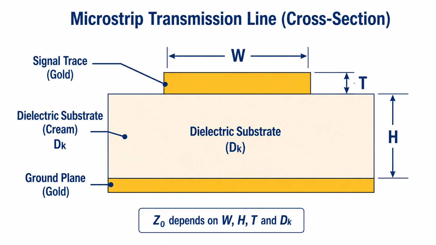
For microstrip (signal trace on outer layer above a ground plane), 50Ω trace width is determined by four parameters:
- Trace width W — the primary design variable
- Substrate height H — distance from trace to ground plane (dielectric thickness)
- Trace thickness T — finished copper thickness after plating
- Dielectric constant Dk — the electrical property of the substrate material
The relationship: wider trace → lower impedance; thicker substrate → higher impedance; higher Dk → lower impedance for same geometry. A 1% change in Dk produces approximately a 0.5% change in impedance. A 10% change in trace width produces approximately a 5–8% change in impedance depending on the W/H ratio.
50Ω Microstrip Trace Width Reference Table
| Material | Dk | Core Thickness | Copper Weight | 50Ω Microstrip Width (approx.) |
|---|---|---|---|---|
| FR4 | 4.5 | 0.2 mm | 1 oz | ~0.36 mm |
| FR4 | 4.5 | 0.4 mm | 1 oz | ~0.73 mm |
| FR4 | 4.5 | 1.0 mm | 1 oz | ~1.85 mm |
| RO4350B | 3.48 | 0.254 mm | 1 oz | ~0.56 mm |
| RO4350B | 3.48 | 0.508 mm | 1 oz | ~1.14 mm |
| RO4003C | 3.38 | 0.305 mm | 1 oz | ~0.66 mm |
| RO3003 | 3.0 | 0.127 mm | 0.5 oz | ~0.28 mm |
| RO3003 | 3.0 | 0.254 mm | 1 oz | ~0.60 mm |
| RT5880 | 2.20 | 0.254 mm | 1 oz | ~0.74 mm |
| RT5880 | 2.20 | 0.508 mm | 1 oz | ~1.51 mm |
Approximate values from nominal Dk. Confirm with fabricator using production Dk from material lot certificate before finalizing layout.
These values are calculated from standard microstrip formulas using nominal Dk. Always confirm with your fabricator using the actual production Dk from the material certificate before finalizing your layout — see next section.
Why You Must Use Production Dk, Not Nominal Dk
Rogers datasheet Dk values are typical values measured at specific test conditions. The actual Dk of the material lot used in your board varies from the nominal:
- RO4350B: nominal Dk 3.48 ±0.05 — a lot at Dk 3.53 shifts 50Ω trace impedance by approximately +1.5Ω
- RO3003: nominal Dk 3.0 ±0.04 — a lot at Dk 3.04 shifts impedance by approximately +0.7Ω
- FR4: Dk varies 4.2–4.8 depending on glass weave, resin content and frequency
Request the material lot Dk certificate from your fabricator and recalculate trace width from the actual measured value before sending final Gerber files. For ±5% impedance tolerance designs, this step is not optional. See controlled impedance RF PCB guide for the full TDR verification specification.
Solder Mask Effect on 50Ω Impedance
Solder mask over a microstrip RF trace adds dielectric loading that lowers the effective impedance. The magnitude depends on solder mask thickness and Dk (typically 3.3–3.8 for standard green solder mask):
- Standard solder mask (15–25 µm): reduces impedance by approximately 1–3Ω on a 50Ω line
- For ±10% tolerance: solder mask effect is usually within budget — no special treatment needed
- For ±5% tolerance: either specify LSOG (Leave Solder mask Off the Ground plane — actually means leave off RF traces) or account for solder mask in the impedance calculation
To specify solder mask relief over RF traces on the fabrication drawing: add a note ‘No solder mask on RF signal traces on layer [X]’ and open the solder mask layer in Gerber files over the RF trace routing.
Corner and Bend Design Rules
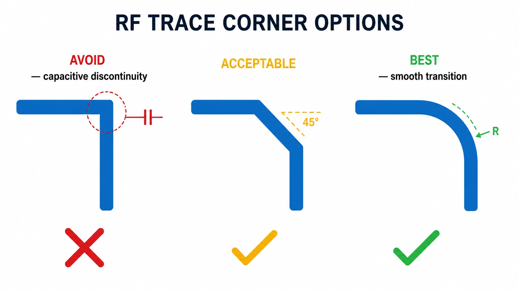
Right-Angle Corners — Avoid
A 90° corner in a RF trace creates an effective capacitive discontinuity — the corner area has more copper width than the trace, increasing local capacitance and lowering local impedance. At frequencies below 1 GHz this effect is negligible. Above 5 GHz, 90° corners produce measurable return loss degradation. At Ka-band (28 GHz), 90° corners are unacceptable.
45° Chamfered Corners — Acceptable
Chamfering the inside corner of a 90° bend reduces the excess copper area by approximately 70%, significantly reducing the capacitive discontinuity. For designs up to 20 GHz, 45° chamfered corners are acceptable in most applications.
Curved Radius Bends — Best
A curved bend with radius ≥3× trace width provides a smooth impedance transition with minimal discontinuity. For mmWave and Ka-band designs above 20 GHz, curved bends are the recommended approach. Most RF PCB EDA tools (ADS, AWR, Sonnet) have curved bend primitives that generate the correct geometry automatically.
Common 50Ω Trace Design Mistakes
| Mistake | Effect on Impedance | Fix |
|---|---|---|
| Using nominal Dk instead of production Dk | ±1–3Ω shift depending on lot variation | Request material Dk certificate, recalculate |
| Solder mask over microstrip not accounted for | –1 to –3Ω (lower impedance) | Specify LSOG over RF traces or include in calc |
| Right-angle corners on RF traces | Capacitive discontinuity at corner | Use 45° chamfer or curved bends |
| Copper pour adjacent to RF trace | Reduces effective impedance | Keep copper pour ≥3× trace width from RF trace |
| Via transition without ground via | Inductance spike at via | Add ground vias adjacent to signal via |
| Specifying ±5% but no TDR on drawing | Factory applies ±10% default | Always specify tolerance explicitly on drawing |
How to Specify 50Ω Impedance on the Fabrication Drawing
A complete impedance specification on the fabrication drawing must include:
- Impedance structure: ’50Ω microstrip on L1, referenced to L2 ground plane’
- Tolerance: ‘±10%’ or ‘±5%’ — must be explicit; default is ±10% if not stated
- Material and thickness: ‘Rogers RO4350B 0.254 mm core, 1 oz finished copper on L1’
- TDR verification required: ‘Yes — TDR verification on every production lot’
- Solder mask note if applicable: ‘No solder mask over RF signal traces on L1’
Without complete specification, the fabricator makes assumptions — and the finished board may not match design intent.
Conclusion
50Ω RF trace width is determined by substrate Dk, dielectric thickness, and copper weight. Always use production Dk from the material lot certificate — not nominal datasheet values. Solder mask reduces impedance by 1–3Ω; specify LSOG over RF traces for ±5% designs. Use 45° chamfers or curved bends — avoid 90° corners above 5 GHz. Specify impedance tolerance explicitly on the fabrication drawing. Riching PCB performs TDR verification on every production lot, provides material Dk certificates on request, and supports ±5% impedance tolerance with panel-level verification. No MOQ. See Rogers materials overview for available materials and thicknesses.
Get a Quote for Your 50Ω RF PCB
RO4350B, RO3003, RT5880 in stock. TDR on every lot. Material Dk certificates on request.
- Gerber files + NC drill file
- Stackup — material, dielectric thickness, copper weight
- Impedance target (50Ω), tolerance (±10% or ±5%), reference layer
- Solder mask relief over RF traces? (yes/no)
- IPC Class and quantity
WhatsApp +86 13760473650— DFM review within 4–8 hours
50 Ohm RF Trace PCB Q&A
Common questions about 50Ω trace width calculation, production vs nominal Dk, solder mask effect, corner design and fabrication drawing specification.
What is the 50 ohm trace width for Rogers RO4350B?
0.254mm core, 1oz copper: ~0.56mm. 0.508mm core, 1oz: ~1.14mm. Calculated from nominal Dk 3.48. Confirm with fabricator using production Dk — lot variation ±0.05 shifts impedance ~±1.5Ω.
Why use production Dk instead of nominal Dk?
RO4350B specified Dk 3.48 ±0.05. A lot at 3.53 shifts trace width ~0.02mm and impedance ~1.5Ω. Within ±10% but approaches ±5% limit. Request material lot Dk certificate, recalculate before finalizing layout.
Does solder mask affect 50Ω RF trace impedance?
Yes — reduces impedance 1–3Ω. For ±10%: usually within budget. For ±5%: specify LSOG (no solder mask over RF traces) on fabrication drawing, or include mask Dk and thickness in impedance calculation.
Can I use 90° corners on 50Ω RF traces?
Below 1 GHz: negligible effect. Above 5 GHz: capacitive discontinuity, measurable return loss. Above 20 GHz: unacceptable. Use 45° chamfer (up to ~20 GHz) or curved radius bend ≥3× trace width (all RF frequencies).
How do I specify 50Ω impedance on the fabrication drawing?
Include: structure type and reference layer, tolerance (±10% or ±5% — explicit), material and thickness, copper weight, TDR required, solder mask note. Without complete spec, fabricator makes assumptions that may not match design intent.
Request a PCB Quote
Upload your Gerber ZIP file and project requirements. Our engineering team will review your PCB material, stackup, impedance needs, surface finish, and production quantity before quoting.
Please prepare:
- Gerber files in ZIP format
- PCB material or stackup requirements
- Controlled impedance notes if available
- Prototype or batch production quantity
