
Rigid-Flex vs FPC — Choosing the Right Structure
Before designing the stackup, confirm whether you need rigid-flex or FPC. FPC (flexible PCB) replaces cables between two separate rigid PCBs — the rigid boards are separate assemblies. Rigid-flex combines rigid and flexible sections in a single board, eliminating connectors and improving reliability in high-vibration environments. The choice affects cost, assembly process and reliability — see rigid flex PCB manufacturer for a full comparison.
Bend Radius Rules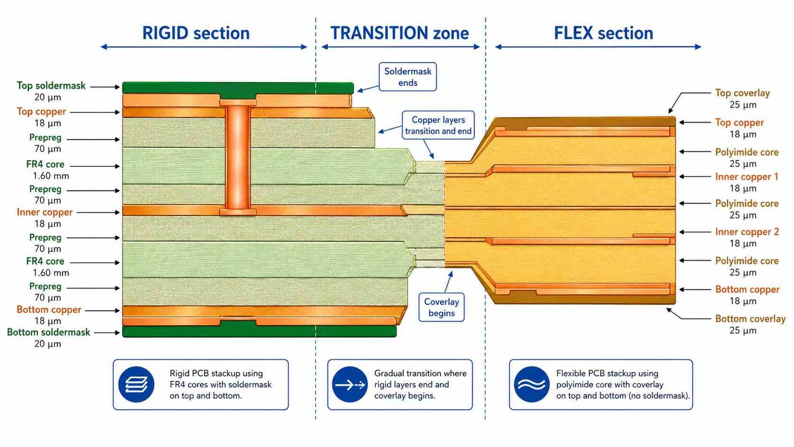
Static vs dynamic bending
Static bending means the flex section is bent once during assembly and remains in a fixed position. Dynamic bending means the flex section bends repeatedly during the product’s life — hinge applications, cable replacement where repeated flexing occurs. Dynamic applications require a larger minimum bend radius (10× flex thickness vs 6× for static) and should use rolled-annealed (RA) copper rather than electrodeposited (ED) copper for fatigue resistance.
How to measure bend radius
Bend radius is measured from the neutral axis of the flex section to the inner surface of the bend — not the outer surface. For a flex section with thickness T, bending it around a radius R produces a strain on the outer copper of approximately T/(2R). At the minimum bend radius of 6×T, outer surface strain is approximately 8.3% — within the fatigue limit for ED copper in static applications.
Layer Stackup for Rigid-Flex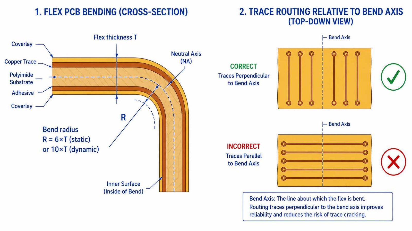
Rigid section stackup
The rigid sections use standard FR4 or high-Tg FR4 construction — copper layers, prepreg, core, soldermask. For rigid-flex with RF content on the rigid sections, Rogers or PTFE materials can be used in the rigid sections with polyimide flex layers bonded using Rogers 4450F bondply.
Flex section stackup
The flex sections use polyimide (PI) substrate with adhesive-bonded copper foil or direct-bond copper. Coverlay (PI film + adhesive) replaces soldermask on the flex sections — soldermask is too rigid for reliable flex applications and will crack on bending. Coverlay openings must clear pad edges by at least 0.3mm.
Transition zone
The transition between rigid and flex sections is a critical stress concentration point. Key rules: do not terminate all layers at the same point (stagger layer drop-offs), add copper relief at the transition, and ensure the first bend starts at least 0.5mm from the rigid-flex boundary.
Trace Routing in the Flex Zone
- Route traces perpendicular to the bend axis — never parallel. Parallel traces experience maximum stress during bending.
- Avoid 45° or curved routing in the bend zone — use straight perpendicular traces only
- Increase trace width by 20–30% in the bend zone to reduce current density and stress
- No vias in the bend zone — vias are rigid stress concentrators and will crack under repeated bending
- Use hatched/mesh copper fills in the bend zone — solid copper fills prevent flexing and cause cracking
- Add teardrop reliefs at trace entry into pads near the flex zone
Coverlay vs Soldermask
Soldermask is a rigid epoxy — it cracks on bending and is not acceptable for the flex sections of a rigid-flex design. Coverlay (polyimide film + adhesive) is flexible and is the standard protective coating for flex sections. Soldermask is used on the rigid sections only. Some manufacturers use flexible soldermask on flex sections as a cost reduction — this is generally not acceptable for dynamic bend applications or IPC Class 3.