
Rogers RO4350B PCB Design Guide — Impedance, Trace Width and When to Upgrade to PTFE
Rogers RO4350B is the most widely used RF PCB substrate in the world — a hydrocarbon ceramic laminate with Dk 3.48 and Df 0.0037, processing on standard FR4-compatible equipment without plasma activation. This guide covers the practical design parameters engineers need when working with RO4350B: 50Ω trace width by thickness and copper weight, insertion loss by frequency, via design rules, hybrid stackup options, and the exact frequency threshold where RO4350B should be replaced with RO3003 or RT5880.
Home » Rogers RO4350B PCB Design Guide — Impedance, Trace Width and When to Upgrade to PTFE
Table of Contents
RO4350B Material Properties
| Property | RO4350B Value |
|---|---|
| Dielectric constant Dk (10GHz) | 3.48 ±0.05 |
| Dissipation factor Df (10GHz) | 0.0037 |
| Thermal conductivity | 0.69 W/m·K |
| CTE (x,y) | 17 ppm/°C — matched to copper |
| Tg (glass transition) | 280°C — compatible with lead-free SAC305 reflow |
| Process compatibility | ✅ FR4-compatible — no plasma activation required |
| Max lamination cycles | 3 cycles (vs 2 for PTFE) |
| Moisture absorption | 0.06% |
| Available bonding prepreg | RO4450F (for RO4350B hybrid stackups) |
The key advantage of RO4350B over PTFE materials is process compatibility: it drills, laminates and plates on the same equipment as FR4, requires no plasma activation, and allows up to 3 lamination cycles. This makes it 2–3× lower cost and 2–3 days faster than RO3003 at prototype quantities. The tradeoff is Df 0.0037 vs 0.0010 for RO3003 — acceptable below 18GHz, problematic above 20GHz.
50Ω Microstrip Trace Width Reference
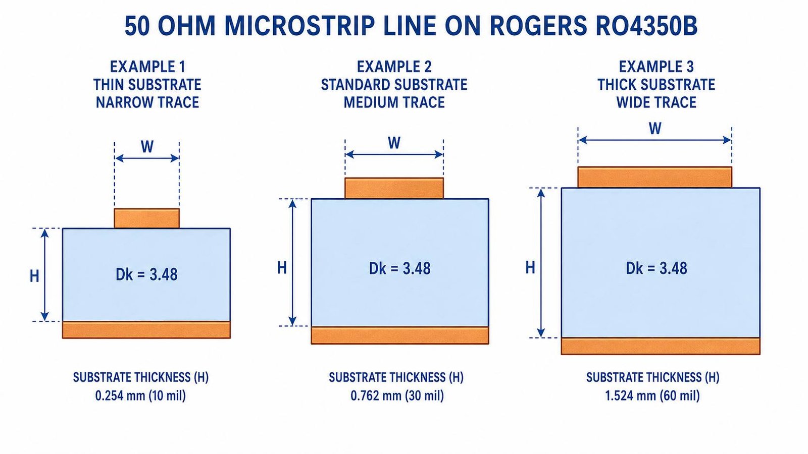
| Substrate Thickness | 0.5oz copper | 1oz copper | 2oz copper | Notes |
|---|---|---|---|---|
| 0.254mm (10mil) | ~0.54mm | ~0.43mm | ~0.30mm | Thin — stripline inner layers |
| 0.338mm (13.3mil) | ~0.74mm | ~0.60mm | ~0.42mm | Common for X-band designs |
| 0.508mm (20mil) | ~1.12mm | ~0.92mm | ~0.65mm | Most common RF thickness |
| 0.762mm (30mil) | ~1.68mm | ~1.40mm | ~1.00mm | Lower frequency / power |
| 1.524mm (60mil) | ~3.36mm | ~2.82mm | ~2.05mm | Very low frequency or high power |
Values calculated for RO4350B Dk 3.48 using IPC-2141A microstrip formula. Actual trace width should be verified against your simulation tool using the measured Dk from the material certificate — RO4350B Dk tolerance is ±0.05, which shifts 50Ω trace width by approximately ±1.5% at 0.508mm substrate thickness.
Dk variation with frequency — use the right value
RO4350B Dk is not constant across frequency. At 1GHz, Dk ≈ 3.66. At 10GHz, Dk ≈ 3.48. At 20GHz, Dk ≈ 3.40. For designs where electrical length matters — filter resonators, antenna patches, delay lines — always use the Dk value at the operating frequency, not the 1GHz value that appears in some datasheets. Using Dk 3.66 at 10GHz in your simulation will produce a trace that is approximately 3% too narrow, shifting your filter center frequency by the same amount.
Insertion Loss by Frequency
| Frequency | RO4350B (dB/cm) | RO4003C (dB/cm) | RO3003 (dB/cm) | 10cm path (RO4350B) |
|---|---|---|---|---|
| 1 GHz | ~0.05 | ~0.04 | ~0.02 | ~0.5 dB |
| 5 GHz | ~0.12 | ~0.09 | ~0.04 | ~1.2 dB |
| 10 GHz | ~0.18 | ~0.13 | ~0.05 | ~1.8 dB |
| 18 GHz | ~0.28 | ~0.20 | ~0.08 | ~2.8 dB ⚠️ |
| 28 GHz | ~0.45 | ~0.32 | ~0.12 | ~4.5 dB ❌ |
| 40 GHz | ~0.65 | ~0.47 | ~0.17 | ~6.5 dB ❌ |
Loss values are approximate for 50Ω microstrip on 0.508mm substrate with 1oz copper. Actual loss depends on copper surface roughness — RO4350B is available with standard electrodeposited (ED) copper and with lower-roughness rolled-annealed (RA) copper. RA copper reduces conductor loss by approximately 20% above 10GHz and is recommended for designs above 15GHz on RO4350B.
Via Design on RO4350B
Through-hole via
- Minimum drill: 0.2mm mechanical (0.1mm laser for buried/blind)
- Via pad: drill + 0.2mm minimum annular ring
- Anti-pad (clearance): via pad + 0.15mm each side minimum
- Via fence for ground isolation: spacing ≤ λ/20 at operating frequency
- At 10GHz: λ/20 ≈ 1.5mm spacing between fence vias
- At 28GHz: λ/20 ≈ 0.54mm spacing — requires laser-drilled vias for fence
Via stub — when backdrill is required
Via stubs act as λ/4 resonators, creating a notch in the transmission response at the frequency where the stub length equals λ/4. For a 1mm stub in RO4350B (Dk 3.48), the notch appears at approximately 40GHz. For designs above 20GHz, stub length should be minimized or backdrill specified to remove the stub. For designs below 15GHz, via stub effect is typically negligible for stub lengths under 2mm.
Hybrid Stackup — RO4350B with FR4
For multilayer designs with RF signal layers and digital/power layers, RO4350B can be combined with FR4 inner layers using RO4450F bondply at the material interface. This reduces cost compared to an all-Rogers stackup while maintaining RF performance on the signal layers.
- RO4350B outer layers (RF signal) + FR4 inner layers (digital/power)
- Bonding film: RO4450F bondply — not standard FR4 prepreg
- Maximum lamination cycles: 3 (set by RO4350B — less restrictive than PTFE’s 2 cycles)
- CTE mismatch: RO4350B x-y CTE 17 ppm/°C ≈ FR4 17 ppm/°C — well matched, minimal stress
- Cost saving vs all-Rogers: typically 30–50% depending on layer count
When to Upgrade from RO4350B to RO3003 or RT5880
| Frequency | Recommendation | Reason |
|---|---|---|
| <5GHz | RO4350B or Hi-Tg FR4 | Loss negligible, cost advantage significant |
| 5–12GHz | RO4350B | Standard choice — loss acceptable, FR4-compatible process |
| 12–18GHz | RO4350B or RO4003C | Verify loss budget per design — RO4003C if margin is tight |
| 18–28GHz | RO4003C or RO3003 | RO4350B loss 3–5 dB over 10cm — unacceptable for most receivers |
| 28GHz+ | RO3003 or RT5880 | RO4350B not viable — PTFE required |
| 2–18GHz wideband EW | RT5880 | Lowest Df across full band |
The loss budget calculation
Before specifying PTFE, calculate your actual loss budget. RO4350B at 18GHz loses approximately 0.28 dB/cm. If your longest RF trace is 5cm, total dielectric loss is 1.4 dB. If your system noise figure budget can absorb 1.4 dB before the LNA, RO4350B is adequate. If you are feeding directly into a low-noise amplifier where every 0.1 dB of NF matters, RO3003 (0.08 dB/cm at 18GHz, total 0.4 dB over 5cm) preserves 1 dB of system NF — which may be worth the 2–3× material cost premium.
The assembly compatibility advantage
RO4350B Tg is 280°C — fully compatible with standard SAC305 lead-free reflow profiles peaking at 255–260°C. No modified reflow profile is required, no risk of dimensional shift during SMT, no special assembly process. This is a significant advantage over PTFE materials (RO3003, RT5880) where the reflow profile must be modified to stay below PTFE’s softening point. For designs where assembly complexity matters — medical devices, automotive electronics requiring IATF16949 traceability — RO4350B’s assembly compatibility is a real engineering advantage, not just a cost argument.
Rogers RO4350B PCB Design — Q&A
Common questions about RO4350B trace width, frequency range, plasma activation, hybrid stackup bonding film and when to upgrade to PTFE materials.
What is the 50Ω trace width for Rogers RO4350B at 0.508mm thickness?
For RO4350B at 0.508mm thickness: approximately 1.12mm with 0.5oz copper, 0.92mm with 1oz copper, and 0.65mm with 2oz copper. Verify in simulation using the measured Dk from your material certificate — RO4350B Dk tolerance is ±0.05.
What frequency is Rogers RO4350B suitable for?
RO4350B (Df 0.0037) is suitable up to approximately 18GHz. Below 12GHz it is the standard choice. Between 12–18GHz, verify your loss budget. Above 18GHz, insertion loss becomes problematic — at 28GHz a 10cm trace loses ~4.5dB, unacceptable for most receivers. Use RO3003 or RT5880 above 20GHz.
Does Rogers RO4350B require plasma activation?
No. RO4350B is a hydrocarbon ceramic laminate, not PTFE. It processes on standard FR4-compatible equipment without plasma activation, allows up to 3 lamination cycles, and is compatible with standard SAC305 lead-free reflow (Tg 280°C). This is a key advantage over PTFE materials like RO3003 and RT5880.
What bonding film is used for Rogers RO4350B hybrid stackups?
Rogers RO4450F bondply is used for RO4350B + FR4 hybrid stackups. Do not use standard FR4 prepreg at this interface. Note: RO4450F is different from Rogers 2929 bondply, which is used for PTFE hybrid stackups (RO3003, RT5880).
When should I upgrade from RO4350B to RO3003?
Upgrade when your operating frequency exceeds 18–20GHz, or when your loss budget shows RO4350B's Df 0.0037 consumes too much system noise figure. At 28GHz, RO4350B loses ~4.5dB over 10cm vs ~1.2dB for RO3003 — a 3.3dB difference that typically exceeds receiver margin. Below 18GHz, RO4350B is adequate and 2–3× less expensive.
RO4350B, RO4003C, RO3003 and RT5880 — All In Stock
Whatever frequency your design operates at, Riching PCB stocks the right material. RO4350B and RO4003C: 5–7 day prototype. RO3003 0.127mm and 0.254mm: 7–10 days. RT5880 in 6 thicknesses: 7–10 days. No MOQ.
Rogers PCB Manufacturer → WhatsAppRequest a PCB Quote
Upload your Gerber ZIP file and project requirements. Our engineering team will review your PCB material, stackup, impedance needs, surface finish, and production quantity before quoting.
Please prepare:
- Gerber files in ZIP format
- PCB material or stackup requirements
- Controlled impedance notes if available
- Prototype or batch production quantity