Through-hole vias in multilayer PCB create an unwanted section of copper that extends beyond the last connected layer — known as a via stub. At low frequencies, this stub has little effect. At high frequencies above 1–2 GHz, the stub acts as a short transmission line resonator and causes signal reflection, insertion loss, and resonance notches that can significantly degrade signal quality.
Back drilling — also called controlled depth drilling or stub removal drilling — is a manufacturing process that removes the unwanted via stub by drilling from the opposite side of the board to a controlled depth. It is used in high frequency PCB, microwave PCB, Rogers PCB, high speed digital PCB, and backplane designs where signal integrity above 5 GHz is critical.
This guide explains what via stubs are, when back drilling is needed, the manufacturing specifications and tolerances, and what design information must be confirmed before production.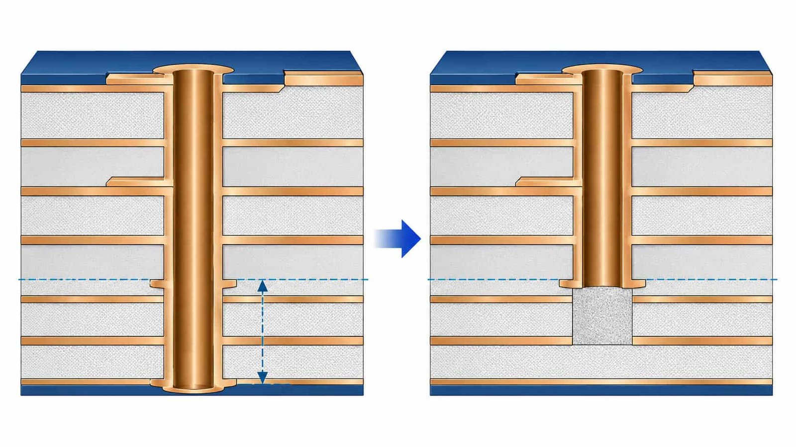
Quick Summary
Key point: Back drilling removes the via stub by controlled-depth drilling from the opposite board surface. Depth tolerance is ±0.1 mm. Remaining stub length after back drilling is ≤ 10 mil. Back drill clearance to the nearest active inner layer copper must be ≥ 6 mil (same net) or ≥ 10 mil (different net). Back drill files must be provided separately from the main drill file.
Back drilling is effective for frequencies above 1–2 GHz where stub resonance begins to affect signal quality. It is commonly used in high frequency RF boards, high speed SerDes channels, backplane connectors, and multilayer microwave PCB where blind vias are not feasible due to board thickness or cost constraints.
What Is a Via Stub and Why Does It Cause Problems?
When a through-hole via is drilled in a multilayer PCB, it passes through every layer from top to bottom. The signal may only need to travel from, for example, the top layer to layer 4. The remaining copper in the via below layer 4 — from layer 4 to the bottom — serves no signal purpose. This unused section is the via stub.
Why the Stub Is a Problem at High Frequencies
The via stub acts as a quarter-wave resonator stub in the signal path. At the frequency where the stub is exactly one quarter of the signal wavelength, the stub presents a near-short circuit to ground, creating a deep notch in the frequency response. This resonance frequency depends directly on the physical stub length.
- Shorter stubs resonate at higher frequencies — less impact in the operating band
- Longer stubs resonate at lower frequencies — more likely to fall within the operating band
- A stub of 100 mil length causes resonance around 15–18 GHz depending on the dielectric
- A stub of 200 mil length causes resonance around 7–9 GHz
- A stub of 400 mil or more causes resonance below 5 GHz, affecting many RF and high speed applications
Rule of thumb: If the via stub length in mils multiplied by the operating frequency in GHz exceeds approximately 1500–2000, stub resonance should be considered. Above this threshold, back drilling or blind vias should be evaluated.
Stub Resonance vs Operating Frequency
For high frequency PCB applications, the threshold where stub effects become significant depends on both stub length and signal frequency. In general:
- Signals below 1 GHz: stubs rarely cause problems except in very thick boards
- Signals at 1–5 GHz: stubs in thick boards (>2.4 mm) begin to affect signal quality
- Signals at 5–15 GHz: stubs of any meaningful length cause measurable insertion loss and reflection
- Signals above 15 GHz: even short stubs can affect performance; back drilling or blind vias are strongly recommended
What Is Back Drilling and How Does It Work?
Back drilling is a controlled-depth mechanical drilling process performed after the board has been drilled, plated, and built up. A slightly larger drill bit is used to drill from the opposite side of the board into the via hole to a controlled depth, removing the copper tube of the via stub.
The back drill does not pass through the entire board — it stops at a controlled depth that leaves a small remaining stub of ≤ 10 mil. This tiny remaining stub is short enough that its resonance frequency is well above the operating band of most RF and high speed applications.
Back Drill vs Blind Via for Stub Removal
Both back drilling and blind vias can address the via stub problem, but they are suited to different situations:
- Back drilling: lower cost than HDI blind vias, applicable to any through-hole via in any layer count, does not require additional lamination cycles, effective for large-diameter connector vias and backplane designs
- Blind vias: no stub at all (not just reduced), suitable for fine-pitch vias and compact RF modules, requires additional lamination cycles and HDI process, higher cost than back drilling
- Back drilling is preferred when: board thickness is large, via diameter is relatively large, cost must be controlled, or the design already uses through-hole vias for other layers
- Blind vias are preferred when: zero stub is required, via pitch is very tight, or the design is already using HDI for other reasons
For blind via design rules and specifications, see Blind and Buried Via Capabilities in High Frequency PCB Manufacturing.
Back Drill PCB Manufacturing Specifications
The table below summarizes key manufacturing specifications for back drilling in high frequency PCB production.
Parameter | Standard Capability | Advanced Capability |
Back drill hole diameter range | 0.4–6.35 mm (drill) | 0.4–6.35 mm (drill) |
Back drill depth tolerance | ±0.1 mm | ±0.1 mm |
Min. stub length remaining (STUB) | ≤ 10 mil | ≤ 10 mil |
Back drill to inner layer clearance | ≥ 6 mil (same net) | ≥ 6 mil (same net) |
Back drill to inner layer clearance (diff. net) | ≥ 10 mil | ≥ 10 mil |
Applicable board thickness | 0.3–5.4 mm | 0.3–5.4 mm |
Max. panel size | 660 × 800 mm | 660 × 800 mm |
Note: Back drill depth tolerance of ±0.1 mm is the critical parameter for stub control. The stub length remaining after back drilling (≤ 10 mil) determines the highest resonance-free frequency. Back drill clearance to active inner layers must be confirmed during stackup review to avoid damaging signal connections.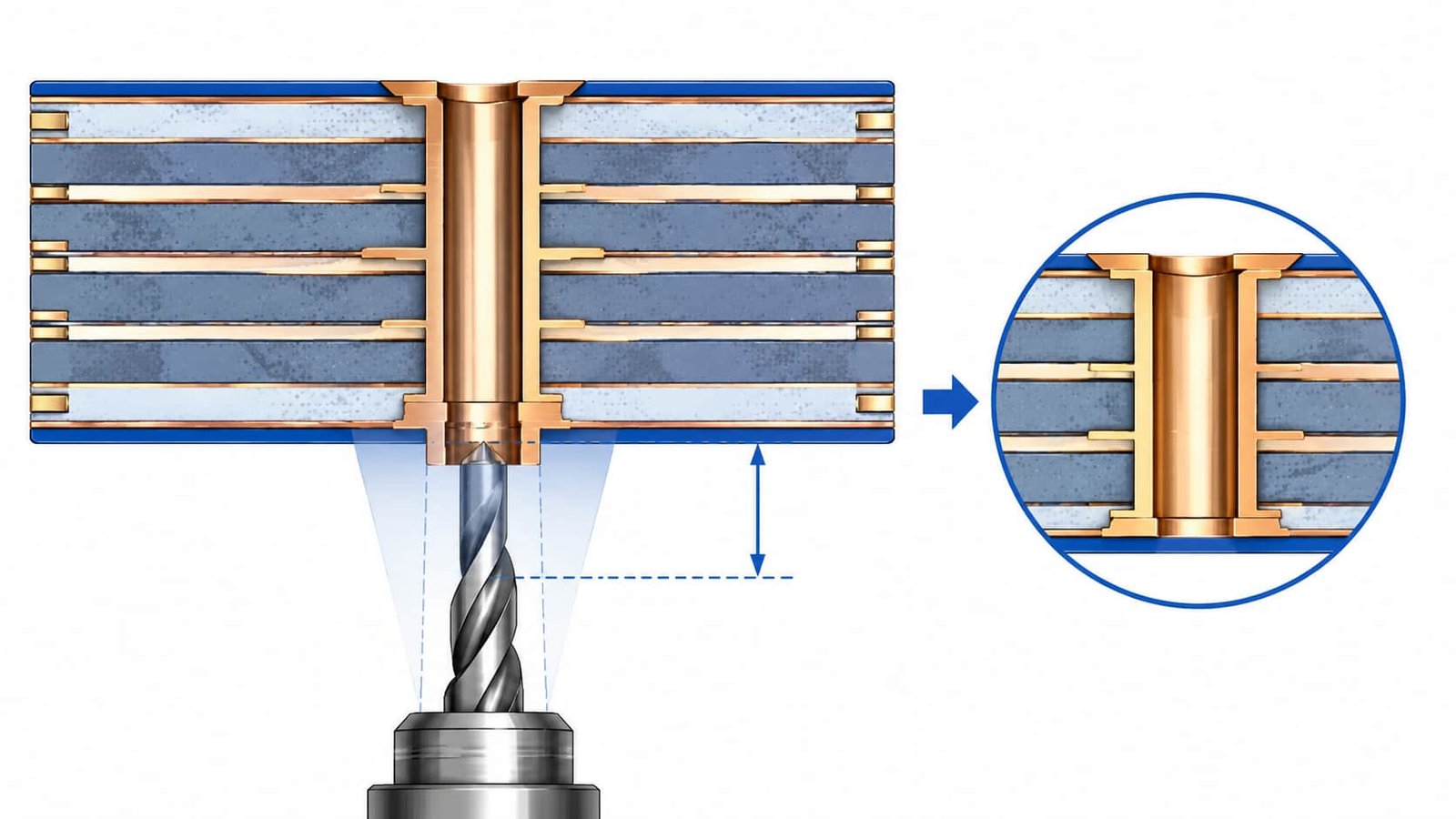
Back Drill Depth Tolerance and Stub Length Control
The back drill depth tolerance of ±0.1 mm is the most critical manufacturing parameter. This tolerance determines how consistently the remaining stub length can be controlled across all vias on the board.
How Depth Tolerance Affects Stub Length
If the target back drill depth leaves a 10 mil (0.254 mm) stub, and the depth tolerance is ±0.1 mm (±3.94 mil), the actual stub length may vary between approximately 6 mil and 14 mil across the board. For most RF and high speed applications, this variation is acceptable.
However, if the target stub is already very short — for example, when the back drill must stop very close to an active inner layer — the depth tolerance becomes more critical. The designer must ensure the back drill stop point is far enough from the nearest active copper to avoid damaging the signal connection even at the worst-case tolerance limit.
Minimum Clearance to Active Inner Layer
The back drill must not damage the copper pad or trace of the nearest active inner layer. Clearance requirements are:
- Same network (same signal): minimum ≥ 6 mil between back drill edge and inner layer copper
- Different network (different signal): minimum ≥ 10 mil between back drill edge and inner layer copper
These clearances must be confirmed in the stackup during engineering review. If the clearance is too tight, back drilling may not be feasible for that via, and blind vias or design changes should be considered.
Design tip: When placing the signal connection layer for a back-drilled via, leave as much distance as possible between the connection layer and the opposite board surface. More distance means more tolerance margin between the back drill stop point and the active copper.
Back Drilling and Signal Integrity for RF PCB
Back drilling improves signal integrity primarily by eliminating the resonance notch caused by stub reflection. The improvement depends on the original stub length, the operating frequency, and the signal type.
Frequencies Where Back Drilling Helps Most
- 5–15 GHz RF and microwave circuits: significant reduction in insertion loss and reflection at stub resonance frequency
- High speed SerDes at 10–56 Gbps: stub resonance often falls within the signal bandwidth; back drilling is commonly specified
- Radar electronics at 24 GHz, 77 GHz: short stubs essential; back drilling used alongside tight via geometry
- Backplane connectors: large via diameter and board thickness make stubs long; back drilling is a standard process
Limitations of Back Drilling
- Remaining stub of ≤ 10 mil still has a resonance frequency — typically above 50 GHz for most board thicknesses
- Back drill depth tolerance ±0.1 mm means stub length varies slightly across the board
- Cannot be applied to vias that are too close to the board edge or to each other
- Back drilling adds a manufacturing process step and increases cost and lead time compared to standard through-hole drilling
- Not a substitute for blind vias in fine-pitch HDI designs
For overall signal integrity review in RF PCB, see Why RF PCB Fails Impedance Testing and Why Microwave PCB Signal Loss Increases After Fabrication.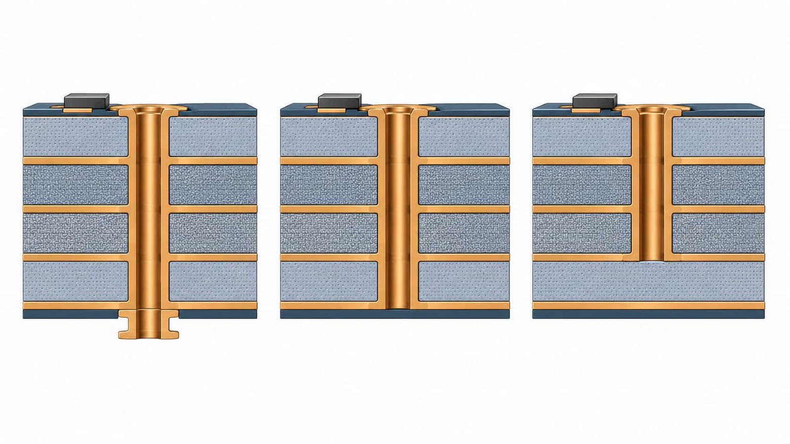
When Should You Specify Back Drilling for High Frequency PCB?
Back drilling should be considered when the following conditions are present:
Signal Frequency Above 5 GHz
For signals above 5 GHz, via stub resonance is likely to fall within or near the operating band for typical multilayer board thicknesses of 1.6 mm and above. Back drilling is strongly recommended unless the design uses blind vias throughout.
Board Thickness Greater Than 1.6 mm
Thicker boards produce longer stubs for any given via connection depth. A 3.2 mm board with a connection at layer 4 of 8 layers will have a stub length of roughly half the board thickness — approximately 1.6 mm (63 mil). This stub length creates resonance around 4–5 GHz, directly affecting many RF applications.
High Speed Digital Signals Above 10 Gbps
High speed SerDes interfaces including 10G, 25G, 56G, and 112G Ethernet, PCIe Gen 4/5, and similar standards have signal bandwidths that overlap with typical via stub resonance frequencies in multilayer boards. Back drilling is widely specified for these interfaces.
RF Connector Vias in Thick Boards
SMA, MMCX, and other RF connector vias in thick multilayer boards often connect only the top or bottom layers, leaving a long stub through the full board thickness. Back drilling the connector vias can significantly improve connector return loss and insertion loss.
For RF connector via design considerations, see Drilling Capabilities for High Frequency PCB: Minimum Hole Size, Aspect Ratio and Tolerances.
Back Drill Design File Requirements
Back drilling requires a separate drill file in addition to the standard NC drill file. Without a properly prepared back drill file, the manufacturer cannot determine which vias to back drill, from which side, and to what depth.
Required Back Drill File Information
- Separate back drill file (not mixed with standard drill file)
- Via coordinates for each back-drilled hole
- Back drill diameter for each via (typically 0.2–0.3 mm larger than the through-hole drill diameter)
- Back drill depth or target layer for each via
- Back drill side (top or bottom)
- Remaining stub length target or stop layer
Stackup Information Required
- Complete stackup with layer sequence, dielectric thickness, and copper weight
- Signal connection layer for each back-drilled via
- Clearance from back drill stop point to nearest active inner layer copper
- Board thickness tolerance
- Controlled impedance requirements for vias in RF signal paths
For a complete file checklist, see What Files Are Needed for a High Frequency PCB Quotation?.
Back Drilling on Rogers and PTFE High Frequency Materials
Back drilling is compatible with most Rogers and PTFE high frequency materials used in RF and microwave PCB, but the softer nature of PTFE materials requires careful process control during back drilling, similar to the considerations for standard through-hole drilling.
- Rogers RO4350B, RO4003C, and hydrocarbon ceramic materials: back drilling is compatible with standard process parameters
- Rogers RT5880, RO3003, and PTFE-based materials: softer material requires adjusted drill parameters to prevent hole wall deformation
- Hybrid FR4 + Rogers stackups: back drill depth must be calculated based on the actual stackup thickness, not nominal values
- F4B and Taconic PTFE materials: follow PTFE-specific process parameters
For PTFE drilling process requirements, see PTFE PCB Manufacturing Challenges and Process Considerations. For hybrid stackup considerations, see FR4 + Rogers Hybrid PCB Stackup: When Should You Use It?.
Information Needed for Back Drill PCB Quotation
To review feasibility and quote accurately, the following information should be prepared:
- Gerber files (all layers)
- Standard NC drill file
- Separate back drill file with drill coordinates, diameter, depth, and side
- Complete PCB stackup with all layer thicknesses and materials
- Signal connection layer for each back-drilled via
- Clearance from back drill stop to nearest active inner layer
- Material type — Rogers, PTFE, Taconic, F4B, or hybrid
- Layer count and total board thickness
- Controlled impedance requirements
- Surface finish
- Quantity — prototype or batch
- Working frequency or application background
[ IMAGE 4 ]
Conclusion
Back drilling is an effective and cost-efficient way to remove via stubs in multilayer high frequency PCB without requiring HDI blind via processes. It is most valuable for RF and microwave circuits operating above 5 GHz, high speed digital signals above 10 Gbps, RF connector vias in thick boards, and backplane designs with long stub lengths.
Manufacturing specifications include a back drill depth tolerance of ±0.1 mm, remaining stub length of ≤ 10 mil, and minimum clearance of ≥ 6–10 mil to active inner layer copper. A separate back drill file and complete stackup information are required before production can be reviewed. Early engineering review with your high frequency PCB manufacturer reduces stub-related signal integrity risk and improves prototype and batch production results.