
Phased Array PCB Design Guide — Element Spacing, Feed Network and Dk Uniformity
Phased array PCB design introduces constraints that do not appear in single-channel RF design: element-to-element phase consistency across the full aperture, feed network amplitude and phase balance across many ports, and substrate Dk uniformity across a potentially large panel area. A 10° phase error between adjacent elements degrades sidelobe level significantly — and at Ka-band, a 1% Dk variation across a panel produces approximately 0.9° of phase error per 10cm signal path. This guide covers the practical design rules for phased array PCB from S-band to Ka-band. For material availability and stackup options, see phased array PCB manufacturer.
Home » Phased Array PCB Design Guide — Element Spacing, Feed Network and Dk Uniformity
Table of Contents
Element Spacing — Why λ/2 Is the Limit
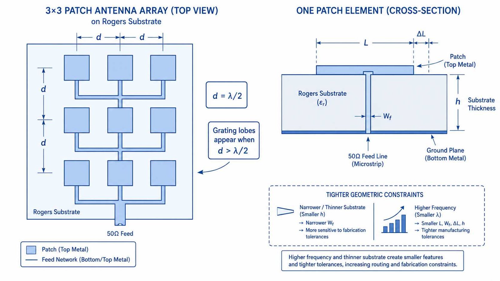
The fundamental constraint on element spacing in a phased array is the grating lobe condition: when inter-element spacing exceeds λ/2 (in free space, or the guided wavelength on the substrate), grating lobes appear in the radiation pattern at scan angles within the visible region. Grating lobes are copies of the main beam at other angles — they reduce directivity and potentially point the array at unintended directions. For a phased array that must scan without grating lobes, element spacing must stay at or below λ/2 at the highest operating frequency.
Element spacing is calculated using free-space λ/2 at the operating frequency — not the guided wavelength on the substrate. The substrate affects the patch element size and feed trace width, not the far-field grating lobe condition.
Element Spacing Reference Table
| Frequency | Free-space λ/2 | On RO3003 (Dk 3.0) | On RO4350B (Dk 3.48) | Notes |
|---|---|---|---|---|
| 3 GHz (S-band) | 50.0mm | 28.9mm | 26.8mm | Large pitch — easier fabrication |
| 10 GHz (X-band) | 15.0mm | 8.66mm | 8.04mm | Standard range |
| 18 GHz (Ku-band) | 8.33mm | 4.81mm | 4.47mm | Trace routing becomes tight |
| 28 GHz (Ka-band) | 5.36mm | 3.09mm | 2.87mm | Feed network width approaches element pitch |
| 40 GHz (Ka-band high) | 3.75mm | 2.17mm | 2.01mm | RO3003 feed barely fits |
| 77 GHz (W-band) | 1.95mm | 1.13mm | 1.05mm | 0.127mm substrate, laser drill required |
The column ‘On RO3003’ and ‘On RO4350B’ shows the effect of substrate Dk on the available space for the feed network within the element pitch — lower Dk (RO3003 Dk 3.0 vs RO4350B Dk 3.48) produces a wider 50Ω trace, which at high frequencies occupies a larger fraction of the available element pitch. This is one reason substrate selection for Ka-band and W-band arrays is constrained by geometry as well as loss.
Substrate Selection by Frequency
| Frequency | Material | Substrate Thickness | Key Reason |
|---|---|---|---|
| 1–6 GHz | RO4350B | 0.508–1.524mm | Loss acceptable, wider trace fits element pitch |
| 6–18 GHz | RO4350B or RO4003C | 0.254–0.508mm | Verify loss budget at highest frequency in band |
| 18–40 GHz | RO3003 | 0.254mm | Lower Dk gives wider trace — critical at tight element pitch |
| 40–80 GHz | RO3003 | 0.127mm | 0.127mm required to maintain element pitch at 50Ω trace width |
| 2–18 GHz wideband | RT5880 | 0.381–0.508mm | Lowest Df across full band — consistent loss at all frequencies |
Each row in this table reflects genuine design constraints — not a ranking of materials by preference. At S-band (3GHz), the element pitch is large enough that trace width and loss are not the limiting factors; at 77GHz, both factors simultaneously constrain the substrate choice to a single combination (RO3003 0.127mm). Do not change substrate without re-running the full impedance and element sizing calculations for your specific design.
Dk Uniformity — The Most Underspecified Parameter
| Material | Dk Tolerance (datasheet) | Phase Error at 28GHz (10cm path) |
|---|---|---|
| Standard FR4 | ±0.2 to ±0.35 | ~5–9° — unusable for most phased arrays |
| Rogers RO4350B | ±0.05 | ~1.3° — acceptable for moderate apertures |
| Rogers RO4003C | ±0.05 | ~1.4° — similar to RO4350B |
| Rogers RO3003 | ±0.04 | ~0.9° — standard for Ka-band arrays |
| Rogers RT5880 | ±0.02 to ±0.04 | ~0.5–1.0° — best available in standard stock |
Panel-level Dk uniformity is the parameter that most directly determines element-to-element phase consistency in a large aperture array. A Dk variation of ΔDk across the panel produces a phase variation in the feed path of approximately:
Δφ ≈ (π × f × L × ΔDk) / (c × √Dk) degrees
where f is frequency in Hz, L is feed path length in meters, and c is the speed of light. For a 10cm feed path at 28GHz on RO3003 (Dk 3.0, ΔDk ±0.04): Δφ ≈ ±0.9°. For FR4 (ΔDk ±0.35): Δφ ≈ ±8°. This is why FR4 is not usable for phased array applications — not primarily because of insertion loss, but because Dk uniformity is insufficient to maintain beam pointing accuracy across a large aperture.
Panel-level vs lot-level Dk variation
Dk uniformity has two components: within-panel variation (Dk across a single production panel) and lot-to-lot variation (Dk between different material batches). For multi-board phased array systems where elements on different boards must maintain phase coherence, request single-lot material for all boards in the array. Even if within-panel Dk is excellent, lot-to-lot variation can introduce systematic phase offsets between boards that the array calibration must compensate.
Corporate Feed Network Design
Wilkinson divider cascade
The most common feed architecture for a passive phased array is a binary tree of Wilkinson power dividers, providing equal amplitude and phase to all elements. At each division level, the two output ports are isolated from each other, reducing the effect of element impedance variations on other elements. The main design constraint is that all path lengths from input to each element must be equal (or differ by integer multiples of λ) to maintain phase coherence. At Ka-band, a path length error of 0.1mm corresponds to approximately 1° of phase error — feed network routing must be length-matched, not just topologically balanced.
Insertion loss accumulation in the feed network
In a corporate feed network with N binary division levels (feeding 2^N elements), the signal passes through N Wilkinson dividers before reaching each element. Each divider introduces insertion loss from the substrate Df, the divider junction discontinuities, and any bends or via transitions in the feed path. This cumulative loss reduces array efficiency and, more importantly, is not uniform — paths with more bends or longer traces to compensate for layout constraints lose more signal than ideal paths, introducing amplitude taper across the aperture that modifies the beam pattern.
DFM Requirements for Phased Array PCB
- Specify Dk uniformity requirement explicitly — e.g. ‘Within-panel Dk variation ≤ ±0.04, single-lot material for all boards in array’
- Feed path length matching: specify tolerance in mm — e.g. ‘±0.1mm feed path length matching between all element ports’
- Trace width tolerance: specify as absolute tolerance — e.g. ‘±0.02mm trace width on all RF feed traces’
- Via fence: specify spacing explicitly — e.g. ‘≤λ/20 via fence spacing around all element feed transitions’
- TDR: specify ±5% on all impedance-controlled traces, with TDR report per panel
- Surface finish: ENIG — patch element dimensional accuracy depends on flat, uniform surface
- Panel registration: specify layer-to-layer registration tolerance — element grid alignment to ground plane directly affects element resonant frequency
Phased Array PCB Design — Q&A
Common questions about element spacing, why FR4 fails for phased arrays, Dk uniformity requirements and feed path length matching tolerances.
What is the element spacing requirement for a phased array PCB?
Element spacing must stay at or below free-space λ/2 at the operating frequency to avoid grating lobes. At 28GHz, λ/2 = 5.36mm. At 77GHz, λ/2 = 1.95mm. The substrate Dk affects patch element size and feed trace width, but the grating lobe condition is determined by free-space wavelength — not guided wavelength.
Why is FR4 not suitable for phased array PCB?
FR4 is unsuitable primarily because of Dk uniformity, not just insertion loss. FR4 Dk varies ±0.2 to ±0.35 across a panel — at 28GHz this produces 5–9° phase error per 10cm feed path, significantly degrading sidelobe performance. Rogers materials with Dk tolerance ±0.04–0.05 produce approximately 0.9–1.3° under the same conditions.
What is the difference between within-panel and lot-to-lot Dk variation?
Within-panel variation affects element-to-element phase consistency on one board. Lot-to-lot variation affects board-to-board consistency in multi-board arrays. For multi-board phased arrays, request single-lot material for all boards to eliminate lot-to-lot variation between array modules.
How tight should feed path length matching be for a Ka-band phased array?
At 28GHz, 0.1mm path length error produces approximately 1° of phase error. For -20dB sidelobe performance, element phase errors should be below 5° RMS — implying feed path matching better than ±0.5mm at 28GHz. Tighter aperture requirements demand tighter tolerances.
Phased Array PCB — RO3003, RO4350B and RT5880 In Stock
Single-lot material available for multi-board array systems. TDR ±5% every panel. Feed path length matching within ±0.1mm. ENIG finish. 7–10 day prototype, no MOQ.
Phased Array PCB Manufacturer → WhatsAppRequest a PCB Quote
Upload your Gerber ZIP file and project requirements. Our engineering team will review your PCB material, stackup, impedance needs, surface finish, and production quantity before quoting.
Please prepare:
- Gerber files in ZIP format
- PCB material or stackup requirements
- Controlled impedance notes if available
- Prototype or batch production quantity