
RF Power Amplifier PCB Design Guide — Thermal Management, Substrate Selection and Grounding
RF power amplifier PCB design combines two sets of constraints that do not usually appear together: RF signal integrity requirements (controlled impedance, low insertion loss, isolation between input and output) and high-power thermal management (heat extraction from the MMIC or transistor die, copper weight for current handling, substrate thermal conductivity). Getting one right while neglecting the other produces a PA PCB that either has poor RF performance or overheats in operation. This guide covers the practical design rules for both dimensions. For Rogers and PTFE material availability, see RF PCB manufacturer.
Home » RF Power Amplifier PCB Design Guide — Thermal Management, Substrate Selection and Grounding
Table of Contents
Substrate Selection for RF PA PCB
| Material | Dk | Df | Thermal Conductivity | PA Application |
|---|---|---|---|---|
| Rogers RO4350B | 3.48 | 0.0037 | 0.69 W/m·K | S/C-band PA below 12GHz — standard choice |
| Rogers RO4003C | 3.38 | 0.0027 | 0.71 W/m·K | Same process as RO4350B, lower Df — verify loss budget |
| Rogers RO3003 | 3.0 | 0.0010 | 0.50 W/m·K | Ka-band PA above 20GHz — PTFE process required |
| Rogers RT5880 | 2.20 | 0.0009 | 0.20 W/m·K ⚠️ | Wideband PA 2–18GHz — lowest loss, lowest thermal conductivity |
| Taconic RF-35 | 3.5 | 0.0018 | 0.26 W/m·K | X-band PA — good loss performance |
| Aluminum PCB (MCPCB) | — | — | 1.0–3.0 W/m·K | High power industrial — not suitable for RF signal layers |
The key tension in PA substrate selection is between Df (which determines insertion loss in the matching networks) and thermal conductivity (which determines how effectively heat moves from the MMIC to the ground plane). Rogers RO4350B (thermal conductivity 0.69 W/m·K) is significantly better than RT5880 (0.20 W/m·K) for thermal management — but RT5880’s lower Df makes it preferable for wideband designs above 6GHz where matching network loss directly affects output power and efficiency. For most narrowband PA designs below 12GHz, RO4350B is the correct starting point.
RT5880’s thermal conductivity (0.20 W/m·K) is approximately 3.5× lower than RO4350B (0.69 W/m·K). In high power density designs where the MMIC junction temperature is critical, this difference matters. Calculate junction temperature with the actual substrate thermal conductivity before selecting RT5880 for a PA application above 5W output power.
Thermal Via Array Design
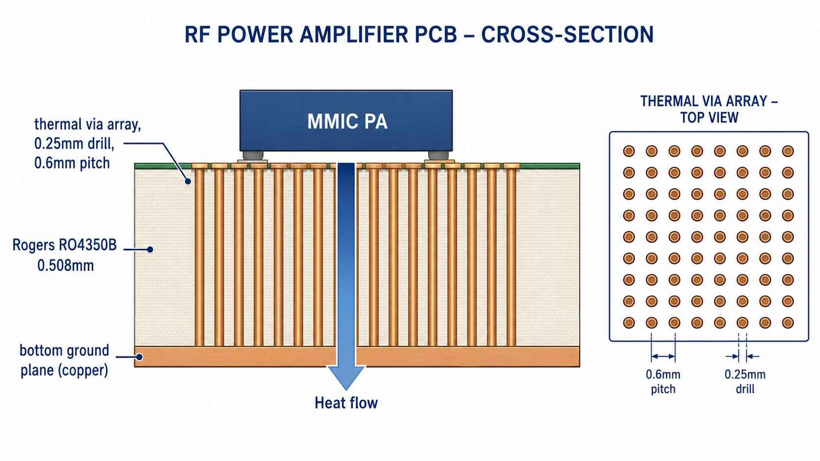
| Parameter | Typical Value | Design Note |
|---|---|---|
| Via diameter | 0.2–0.3mm | Smaller = more vias per area = better thermal, check aspect ratio |
| Via pitch | 0.5–0.8mm center-to-center | Denser array = lower thermal resistance |
| Via fill | Copper fill or resin fill | Copper fill: better thermal. Resin fill: flatter surface for SMT |
| Array coverage | 100% under die attach pad | Full coverage under MMIC/transistor footprint |
| Thermal resistance per via | ~15–25°C/W | 0.25mm drill, 1.6mm board — calculate total from parallel via count |
| Solder mask | Open on both sides | Allows solder wicking for thermal interface |
Junction temperature calculation
The thermal path from MMIC junction to ambient involves three resistances in series: junction-to-case (θJC, specified in the device datasheet), case-to-board (thermal interface material or solder, typically 5–15°C/W), and board-to-ambient (determined by the via array and heatsink). The thermal via array reduces the board-to-ambient resistance by providing low-resistance copper paths from the top copper layer directly to the ground plane and, if mounted on a heatsink, to the heatsink.
For a MMIC dissipating 5W on a 5mm × 5mm package with a 20-via array (0.25mm drill, 0.6mm pitch, 1.6mm board), the thermal resistance of the via array alone is approximately 15°C/W — giving 75°C temperature rise across the via array at 5W dissipation. Adding a bottom-side heatsink reduces this significantly. Increasing via count or decreasing via pitch reduces via array thermal resistance proportionally.
Copper Weight for RF PA PCB
| Copper Weight | Finished Thickness | Insertion Loss Effect | Best For |
|---|---|---|---|
| 0.5oz | ~17μm | Highest conductor loss — avoid for PA output match | Inner signal layers only |
| 1oz | ~35μm | Standard — acceptable to ~18GHz | General RF signal, input match |
| 2oz | ~70μm | Lower conductor loss above 10GHz | PA output match, high current bias feeds |
| 3oz+ | ~105μm+ | Best conductor loss, widest trace for same impedance | Power distribution, DC bias bus |
Copper weight affects both RF performance and power handling. Heavier copper reduces conductor loss in matching networks (beneficial above 5GHz) and reduces resistive loss in bias current paths (beneficial for PA efficiency). The tradeoff: heavier copper changes the 50Ω trace width calculation — a 2oz copper trace for 50Ω on 0.508mm RO4350B is approximately 0.85mm vs 1.05mm for 1oz copper. Recalculate trace width whenever changing copper weight from the simulation assumption.
Grounding Rules for RF PA PCB
| Grounding Requirement | Design Rule |
|---|---|
| MMIC source/emitter ground | Via array directly under die — no trace length between die pad and via |
| Via inductance budget | Each 0.25mm via adds ~0.3nH — at 10GHz this is ~19Ω reactance. Keep via count high, length short |
| Ground plane continuity | No gaps or splits under any RF trace — return current path must be uninterrupted |
| Input/output isolation | Via fence between input and output matching networks — prevents reverse coupling and oscillation |
| Bias line decoupling | Radial stub or quarter-wave choke at each bias feed point — prevents RF from entering DC supply |
| Package ground paddle | All exposed pad ground connections via array to ground plane — not just perimeter pads |
Via inductance — the hidden oscillation risk
Every via in the ground path of a PA adds inductance. For a 0.25mm diameter via through 1.6mm of substrate, inductance is approximately 0.3nH. At 10GHz, 0.3nH presents a reactance of approximately 19Ω — significant compared to the 50Ω system impedance. For a MMIC with 4 source/emitter ground vias, the total ground inductance is approximately 0.075nH (four in parallel), presenting about 4.7Ω at 10GHz. This residual ground inductance can cause instability if the PA has gain above the frequency where the ground inductance starts to appear as positive feedback. Use the maximum practical number of vias under the MMIC package ground pad.
Input/output isolation
Reverse isolation between PA output and input is limited by the device itself, but the PCB layout can add reverse coupling paths through the substrate or through shared ground connections. A via fence between the input and output matching networks — continuous, at ≤λ/10 spacing at the operating frequency — eliminates substrate coupling as a significant reverse path. Shared ground via inductance between input and output paths is another coupling mechanism: use separate via arrays for input and output ground returns wherever practical.
Bias Line Design for RF PA PCB
- Radial stubs or quarter-wave chokes: RF isolation at the bias feed point — prevents RF energy from traveling back into the DC supply and prevents the bias line from acting as an unintended antenna
- Decoupling capacitors: multiple values in parallel (100pF + 10nF + 100nF) at the bias feed point — each value targets a different frequency range
- Bias trace width: size for DC current plus 20% margin — a 1A bias current requires approximately 1mm trace width on 1oz copper for reasonable temperature rise
- Bias line routing: keep bias traces away from the RF signal path — crossing a bias trace over an RF trace creates parasitic coupling that can cause instability
DFM Checklist for RF PA PCB
- Thermal via array: confirm drill diameter, pitch and fill type (copper fill vs resin fill) with fabricator before Gerber submission
- Copper weight: specify finished copper weight per layer explicitly — not starting weight. ‘2oz finished copper on L1’ not ‘2oz copper’
- Via under MMIC pad: confirm solder mask opening matches the thermal pad footprint — soldermask must be open on both sides of via array for solder wicking
- Impedance specification: recalculate 50Ω trace width for the actual copper weight and substrate thickness — not the generic calculator value
- Ground plane continuity: check for any splits or gaps under RF traces in the ground reference layer — common when bias traces or other signals route on the same layer as the ground reference
- Substrate thermal conductivity: confirm the selected material’s thermal conductivity supports the MMIC junction temperature budget before committing to layout
RF Power Amplifier PCB Design — Q&A
Common questions about substrate selection, thermal via array design, via inductance and copper weight for RF PA PCB.
What PCB substrate is best for RF power amplifier design?
Rogers RO4350B (Dk 3.48, Df 0.0037, thermal conductivity 0.69 W/m·K) is the standard starting point for RF PA PCB below 12GHz — acceptable insertion loss with the best thermal conductivity of common RF substrates, FR4-compatible process. For wideband PA above 6GHz where loss is critical, RT5880 (Df 0.0009) offers lower loss but thermal conductivity of only 0.20 W/m·K — verify junction temperature before selecting for high power density designs.
How do I design a thermal via array for a MMIC power amplifier?
Use 0.2–0.3mm drill vias at 0.5–0.8mm pitch, covering 100% of the MMIC die attach pad. Copper-filled vias provide better thermal performance than open or resin-filled. Each 0.25mm via through 1.6mm board gives approximately 15–25°C/W thermal resistance — calculate total from parallel via count. Specify solder mask open on both sides of the via array.
Why does via inductance matter in RF power amplifier PCB?
Each ground via adds approximately 0.3nH inductance. At 10GHz, 0.3nH presents about 19Ω reactance. Residual ground inductance under the MMIC can cause instability via positive feedback. Use maximum practical via count under the package ground pad, placed as close as possible to the die.
What copper weight should I use for RF PA PCB?
1oz finished copper is standard for general RF signal and input matching. 2oz reduces conductor loss in the output matching network above 10GHz and handles higher bias currents. Recalculate 50Ω trace width when changing copper weight — 2oz on 0.508mm RO4350B requires ~0.85mm for 50Ω vs ~1.05mm for 1oz.
RF PA PCB — Rogers RO4350B and RO3003 In Stock, Thermal Via Array Supported
Copper-filled and resin-filled thermal via arrays. 2oz and 3oz copper available. RO4350B 5–7 days, RO3003 7–10 days. TDR impedance verification every lot. No MOQ.
RF PCB Manufacturer → WhatsAppRequest a PCB Quote
Upload your Gerber ZIP file and project requirements. Our engineering team will review your PCB material, stackup, impedance needs, surface finish, and production quantity before quoting.
Please prepare:
- Gerber files in ZIP format
- PCB material or stackup requirements
- Controlled impedance notes if available
- Prototype or batch production quantity