
5G Communication Module PCB Design Guide — Sub-6GHz Material Selection and RF Front-End Layout
5G communication module PCB spans a wider frequency range than any previous cellular generation — from 600MHz low-band through 6GHz mid-band (FR1) to 24–40GHz mmWave (FR2). A single 5G module design rarely needs one substrate for the entire board: the RF front-end, digital baseband, and mmWave antenna sections each have different material requirements. This guide covers substrate selection by 5G band, RF front-end layout considerations, and stackup design for modules that combine sub-6GHz and mmWave sections. For material stock, see Rogers PCB manufacturer and high frequency PCB manufacturer.
Home » 5G Communication Module PCB Design Guide — Sub-6GHz Material Selection and RF Front-End Layout
Table of Contents
5G Frequency Bands and Substrate Requirements
| Band Type | Frequency Range | Typical Module | Substrate Priority |
|---|---|---|---|
| Sub-6GHz low/mid | 600MHz–3.8GHz | Modem, small cell, CPE | FR4 or Hi-Tg FR4 usually sufficient |
| Sub-6GHz high (n77/n78/n79) | 3.3–4.2 / 4.4–5.0GHz | CPE, small cell RF front-end | RO4350B for RF front-end layers |
| mmWave FR2 (n257/n258/n261) | 24.25–29.5GHz | Phased array module, CPE antenna | RO3003 — PTFE required |
| mmWave FR2 (n260) | 37–40GHz | High-band mmWave array | RO3003 0.127mm |
The 3GPP 5G NR standard defines FR1 (sub-6GHz, technically up to 7.125GHz including newer allocations) and FR2 (mmWave, 24.25–52.6GHz). Most commercial 5G modules deployed today use FR1 bands — n77, n78, n79 for mid-band, plus low-band re-farmed from 4G spectrum. FR2 mmWave modules are concentrated in fixed wireless access (FWA), some premium smartphones, and phased array base station equipment.
Insertion Loss Across 5G Bands
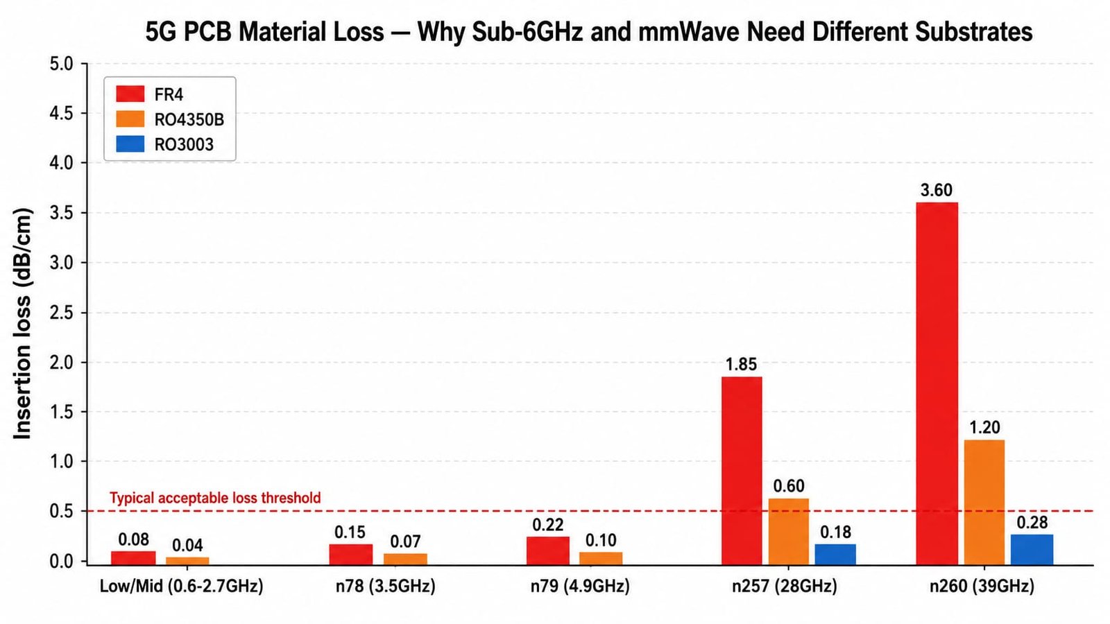
| Frequency (5G band) | FR4 (dB/cm) | RO4350B (dB/cm) | RO3003 (dB/cm) | 10cm trace on RO4350B |
|---|---|---|---|---|
| 0.6–2.7GHz (low/mid) | ~0.03–0.10 | ~0.03–0.06 | — | ~0.3–0.6 dB |
| 3.5GHz (n78) | ~0.14 | ~0.06 | — | ~0.6 dB |
| 4.9GHz (n79) | ~0.19 | ~0.09 | — | ~0.9 dB |
| 28GHz (n257) | ~1.2 | ~0.45 | ~0.12 | ~4.5 dB — often excessive |
| 39GHz (n260) | ~1.7 | ~0.65 | ~0.17 | ~6.5 dB — RO4350B unusable |
The loss data shows why 5G module design is not a single-material problem. At n78 (3.5GHz), standard FR4 already produces measurable insertion loss (~0.14 dB/cm) — for RF front-end sections with filters and power amplifier matching networks, RO4350B’s lower Df (0.0037 vs FR4’s ~0.02) is usually worth the material cost premium. At mmWave frequencies, FR4 and even RO4350B are not viable — PTFE materials like RO3003 are required.
RF Front-End Layout for Sub-6GHz 5G Modules
Filter and PA section on Rogers, digital section on FR4
Most sub-6GHz 5G modules use a hybrid stackup: the RF front-end (filters, PA matching network, antenna switch routing) on RO4350B or RO4003C, with digital baseband and SoC fan-out on standard FR4. This FR4 + Rogers hybrid stackup approach concentrates material cost only where RF performance is needed, keeping the majority of the board (often the larger digital section) on lower-cost FR4.
PA thermal management in compact modules
5G modules are often space-constrained, placing the PA close to digital circuitry and requiring careful thermal design. See RF power amplifier PCB design guide for thermal via array design and copper weight considerations that apply directly to 5G module PA sections.
Ground plane continuity across the RF-digital boundary
Where the RF front-end section transitions to the digital section — even within a single-material board — ground plane continuity must be maintained. A split or gap in the ground reference at this transition creates return current discontinuities that increase EMI coupling between the RF front-end and digital switching noise from the SoC. This is a common source of desense (receiver sensitivity degradation) in compact 5G modules.
mmWave Antenna Module Design (FR2)
For FR2 mmWave modules, the antenna array section requires RO3003 or similar PTFE material — the same design constraints that apply to phased array PCB apply directly: element spacing at λ/2, Dk uniformity across the array panel, and via fence design for element isolation. Most mmWave 5G modules use a hybrid construction — RO3003 antenna array layer bonded to FR4 or RO4350B layers carrying the beamforming IC and digital control circuitry.
Stackup Design Reference
| Layer Function | Typical Material | Design Note |
|---|---|---|
| RF front-end (PA, LNA, filter routing) | RO4350B or RO4003C (sub-6GHz) | FR4-compatible process, standard for most 5G modem RF layers |
| Digital baseband / SoC routing | FR4 or Hi-Tg FR4 | High layer count for BGA fan-out, no RF constraint |
| mmWave antenna module | RO3003 | Required above 24GHz — PTFE process, in-house plasma activation |
| Antenna-to-module transition | Rogers 2929 bondply (if hybrid) | Required at RO3003-to-FR4 interface in hybrid antenna modules |
| Power delivery / ground | FR4 heavy copper | 2oz+ copper for PA current delivery |
Design Checklist for 5G Communication Module PCB
- Confirm which 5G bands the module supports — this determines whether sub-6GHz FR4/Rogers hybrid or mmWave PTFE stackup is required
- Specify impedance control explicitly for RF front-end traces — ±10% standard, ±5% for tight filter or PA matching applications
- Verify ground plane continuity at RF-to-digital section boundaries — no splits under RF signal paths
- For mmWave sections: specify Dk uniformity requirement and TDR verification at multiple panel locations, following phased array design rules
- Specify bonding film explicitly for any hybrid stackup — RO4450F for RO4350B/RO4003C-to-FR4, Rogers 2929 for RO3003-to-FR4
- Confirm thermal via array design for PA sections — compact module thermal margins are tighter than larger board designs
5G Communication Module PCB — Q&A
Common questions about material selection for sub-6GHz vs mmWave 5G modules, FR1/FR2 differences, and stackup design for RF front-end and digital sections.
What PCB material is used for 5G communication module design?
Depends on frequency band. Sub-6GHz RF front-end (n77/n78/n79): Rogers RO4350B or RO4003C — FR4-compatible with acceptable loss. mmWave FR2 (24-40GHz): Rogers RO3003 (PTFE) required. Most modules use hybrid stackup — RF-appropriate material on front-end, standard FR4 for digital baseband.
Can I use standard FR4 for a 5G n78 (3.5GHz) module?
FR4 produces ~0.14 dB/cm at 3.5GHz — acceptable for short traces, but for filter/PA matching networks Rogers RO4350B (~0.06 dB/cm) is standard. Many n78 modules use hybrid construction with RO4350B only on the RF front-end and FR4 for the rest.
What is the difference between FR1 and FR2 in 5G PCB design?
FR1 (sub-6GHz, up to ~7.125GHz) covers most commercial deployment today. FR2 (mmWave, 24.25-52.6GHz) requires PTFE substrates like RO3003 rather than FR4 or hydrocarbon ceramics — FR1 materials are unusable at mmWave loss levels. FR2 modules typically follow phased array antenna design principles.
How is a mmWave 5G antenna module PCB different from a phased array PCB?
Same core principles apply: λ/2 element spacing, Dk uniformity across the panel, via fence isolation. The main difference is integration scale — 5G mmWave modules typically integrate the antenna array with beamforming ICs in a compact form factor, using hybrid stackups combining RO3003 antenna layers with FR4 or RO4350B for beamforming and control circuitry.
5G Module PCB — Sub-6GHz RO4350B and mmWave RO3003 Both In Stock
RF front-end hybrid stackups (RO4350B + FR4) and mmWave antenna modules (RO3003 + FR4) both supported. RO4450F and Rogers 2929 bondply in stock. 5–10 day prototype, no MOQ.
High Frequency PCB Manufacturer → WhatsAppRequest a PCB Quote
Upload your Gerber ZIP file and project requirements. Our engineering team will review your PCB material, stackup, impedance needs, surface finish, and production quantity before quoting.
Please prepare:
- Gerber files in ZIP format
- PCB material or stackup requirements
- Controlled impedance notes if available
- Prototype or batch production quantity