
Rogers PCB vs PTFE PCB: The Decision Engineers Get Wrong Above 20GHz
The most common material selection error in high frequency PCB design is using Rogers RO4350B above 20GHz. RO4350B (Df 0.0037) is an excellent material — but it is a hydrocarbon ceramic, not PTFE, and its insertion loss at 28GHz and above makes it the wrong choice for Ka-band, 77GHz radar and most EW receiver designs. This guide shows exactly where the frequency crossover happens, what it costs in dB, and when PTFE is genuinely necessary vs unnecessary expense.
Home » High Frequency PCB » Rogers PCB vs PTFE PCB: Which Material Is Better for Your Project?
Table of Contents
Key point: Rogers RO4350B is not a PTFE material — it is a hydrocarbon ceramic laminate that processes on standard FR4-compatible equipment. Rogers PTFE materials (RO3003, RT5880, RO3006) require plasma hole wall activation before copper plating, PTFE-specific drill parameters, Rogers 2929 bondply, and a maximum of 2 lamination cycles. The most common mistake is specifying "Rogers PCB" without distinguishing between these two completely different manufacturing processes. Riching PCB stocks both Rogers hydrocarbon and PTFE materials with in-house plasma activation for all PTFE orders.
Rogers PCB vs PTFE PCB — Material Properties
| Property | RO4350B | RO4003C | RO3003 | RT5880 |
|---|---|---|---|---|
| Type | Hydrocarbon ceramic | Hydrocarbon ceramic | PTFE ceramic | PTFE woven glass |
| Dk (10GHz) | 3.48 | 3.38 | 3.0 | 2.20 |
| Df (10GHz) | 0.0037 | 0.0027 | 0.0010 | 0.0009 |
| Insertion loss (10GHz, 10cm) | ~1.8 dB | ~1.3 dB | ~0.5 dB | ~0.45 dB |
| Plasma activation | ✅ Not required | ✅ Not required | ⚠️ Required | ⚠️ Required |
| Prototype lead time | 5–7 days | 5–7 days | 7–10 days | 7–10 days |
| Relative cost | 1× | 1.1× | 2.5–3× | 3–4× |
| Best frequency range | <18GHz | <20GHz | 10–80GHz | 2–40GHz wideband |
The critical distinction: RO4350B and RO4003C are hydrocarbon ceramic laminates — they process like FR4 (no plasma activation required, standard drill parameters, up to 3 lamination cycles). RO3003 and RT5880 are PTFE ceramic composites — they require in-house plasma activation, PTFE-specific drill parameters, and maximum 2 lamination cycles. This process difference directly affects lead time and cost, not just electrical performance.
Insertion Loss by Frequency — Where the Numbers Diverge
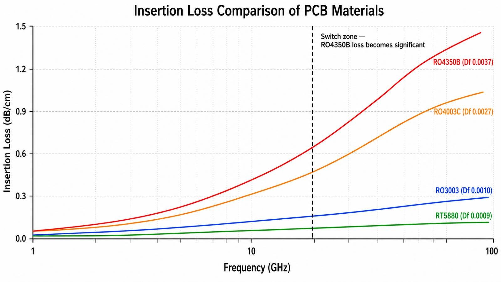
| Frequency | RO4350B (dB/cm) | RO4003C (dB/cm) | RO3003 (dB/cm) | RT5880 (dB/cm) |
|---|---|---|---|---|
| 1 GHz | ~0.05 | ~0.04 | ~0.02 | ~0.018 |
| 5 GHz | ~0.12 | ~0.09 | ~0.04 | ~0.035 |
| 10 GHz | ~0.18 | ~0.13 | ~0.05 | ~0.045 |
| 18 GHz | ~0.28 | ~0.20 | ~0.08 | ~0.07 |
| 28 GHz | ~0.45 | ~0.32 | ~0.12 | ~0.10 |
| 40 GHz | ~0.65 | ~0.47 | ~0.17 | ~0.14 |
| 77 GHz | ~1.4 | ~1.0 | ~0.35 | ~0.28 |
These are approximate values for a 50Ω microstrip trace on standard substrate thickness (0.508mm) with 1oz copper. Actual loss depends on trace geometry, copper roughness grade and thickness. The trend is consistent regardless: below 10GHz the difference between RO4350B and RO3003 is small enough that RO4350B wins on cost and lead time. Above 18–20GHz, RO3003’s advantage grows rapidly and becomes the dominant design driver.
Worked example: 10cm feed network at 28GHz
A 10cm feed network at 28GHz (Ka-band downlink):
- RO4350B: 0.45 dB/cm × 10cm = 4.5 dB insertion loss
- RO3003: 0.12 dB/cm × 10cm = 1.2 dB insertion loss
- Difference: 3.3 dB — equivalent to the receiver NF degradation of a poor LNA
At 77GHz over the same 10cm path: RO4350B produces ~14 dB loss vs ~3.5 dB for RO3003. RO4350B is simply not usable for 77GHz radar front-end designs — this is not a marginal difference, it is a fundamental constraint.
Decision Guide by Frequency and Application
| Frequency | Typical Application | Recommended | Reason |
|---|---|---|---|
| <5GHz | WiFi, IoT, sub-6GHz 5G | RO4350B or Hi-Tg FR4 | Df difference negligible, cost matters |
| 5–12GHz | X-band radar, WLAN, 5G pre-stage | RO4350B / RO4003C | Standard choice, FR4-compatible process |
| 12–20GHz | Ku-band VSAT, 5G mmWave | RO4003C / RO3003 | Loss budget tightening — verify per design |
| 20–30GHz | Ka-band LEO satcom, 28GHz 5G | RO3003 | RO4350B loss too high for most designs |
| 40–80GHz | 77GHz FMCW radar, Ka-band | RO3003 0.127mm | PTFE mandatory, 0.127mm standard for 77GHz |
| 2–18GHz wideband | EW receiver, DRFM, ESM | RT5880 | Lowest Df across full EW band |
The 18–20GHz zone is genuinely ambiguous and depends on trace length, loss budget and system sensitivity. If your feed network is short (<3cm) and you have 2dB margin in the link budget, RO4350B may be acceptable at 20GHz. If your traces are long or margins are tight, RO3003 is the correct choice. When in doubt, run the insertion loss calculation for your specific geometry before committing to material.
The Manufacturing Difference
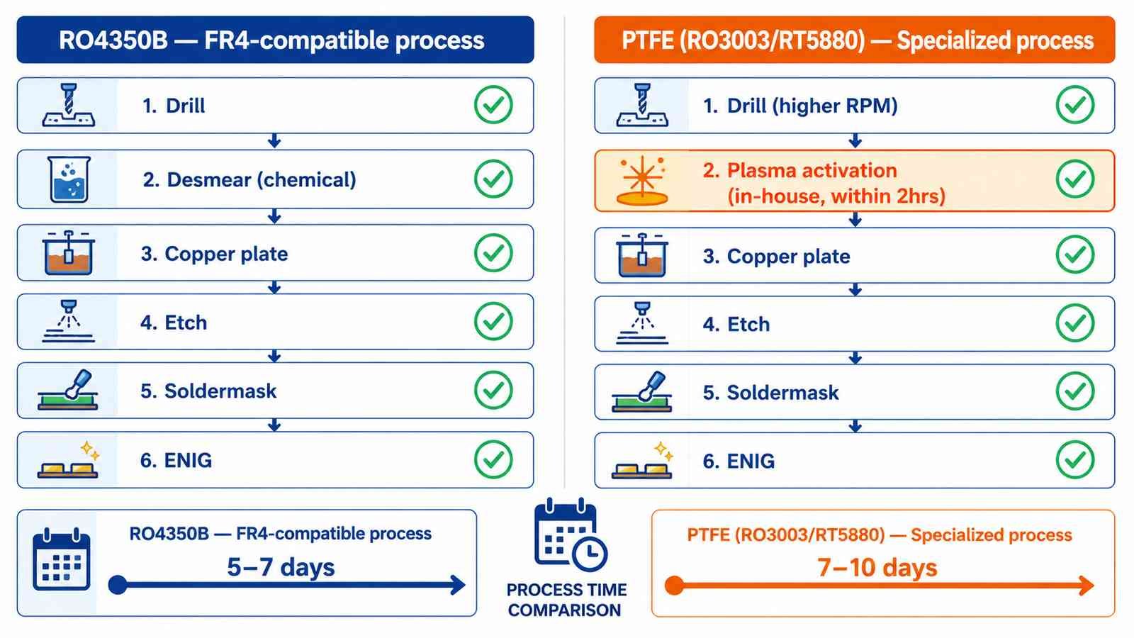
| Process Step | RO4350B / RO4003C | RO3003 / RT5880 (PTFE) |
|---|---|---|
| Drilling | Standard parameters — same as FR4 | PTFE-specific: 40–60K RPM spindle, separate program |
| Hole wall prep | Standard desmear — chemical process | Plasma activation mandatory — electrical discharge etches PTFE surface for copper adhesion |
| Plasma activation | ✅ Not required | ⚠️ In-house only — must occur within 2 hours of copper plating |
| Lamination cycles | Up to 3× press cycles | Max 2× press cycles |
| Impedance control | ±10% standard, ±5% TDR available | ±10% standard, ±5% TDR available |
| Prototype lead time | 5–7 working days | 7–10 working days |
Why plasma activation matters
PTFE is chemically inert — standard chemical desmear does not create the surface roughness needed for reliable copper adhesion on PTFE hole walls. Plasma activation uses an electrical discharge to etch the PTFE surface at the molecular level, creating mechanical interlocking with the electroless copper. Without it, copper peels from hole walls under thermal cycling. In-house plasma activation is the critical process step that separates PTFE-capable factories from those that claim capability but outsource it — outsourcing adds 2–5 days and introduces timing risks (plasma-to-plate window is 2 hours).
Cost implications
RO3003 material costs approximately 2.5–3× more per m² than RO4350B. Combined with the longer fabrication process (7–10 days vs 5–7 days) and tighter process controls, PTFE PCBs typically cost 2–3× more than equivalent RO4350B designs for prototype quantities. For production volumes, the gap narrows but PTFE remains significantly more expensive. This cost premium is justified at frequencies above 18–20GHz where the performance difference is large — and it is not justified below 10GHz where RO4350B’s loss is acceptable.
Hybrid Stackup — When to Use Both
For multilayer designs with RF layers above 20GHz and digital/power layers, a hybrid stackup combining RO3003 RF layers with FR4 inner layers is often the right solution. Rogers 2929 bondply is used at the material interface. The RF layers get PTFE performance; the digital layers get FR4 cost. This is the standard approach for Ka-band phased array modules and 77GHz radar systems where the RF front-end is on PTFE and the signal processing is on FR4.
- RO3003 + FR4 hybrid: RF performance where needed, FR4 cost everywhere else
- Rogers 2929 bondply at material interfaces — in stock at Riching PCB
- Layer count: up to 50 layers including hybrid configurations
- TDR impedance verification on RF layers — ±10% standard, ±5% available
Quick Reference — Which Material for Your Design
- Sub-6GHz (WiFi, IoT, sub-6GHz 5G) → RO4350B or Hi-Tg FR4
- 6–18GHz (X-band radar, Ku-band, microwave backhaul) → RO4350B or RO4003C
- 18–28GHz (Ka-band, 5G mmWave 28GHz) → RO3003 0.254mm
- 28–80GHz (Ka-band radar, 77GHz FMCW) → RO3003 0.127mm
- 2–18GHz wideband (EW, DRFM, ESM) → RT5880 (lowest Df across full band)
- Hybrid multilayer with both RF and digital → RO3003/RT5880 RF layers + FR4 inner layers
Rogers PCB vs PTFE PCB Q&A
Common questions about when to choose Rogers hydrocarbon vs PTFE materials, frequency crossover points, insertion loss comparison, and manufacturing process differences.
What is the difference between Rogers PCB and PTFE PCB?
Rogers PCB is a broad term covering all PCBs made on Rogers Corporation laminates. Some Rogers materials (RO4350B, RO4003C) are hydrocarbon ceramics that process like FR4 — no plasma activation needed. Others (RO3003, RT5880) are PTFE composites that require in-house plasma activation and PTFE-specific drilling. PTFE PCB refers specifically to boards made on PTFE-based substrates, which offer the lowest insertion loss but require specialized fabrication and cost 2–3× more than RO4350B.
When should I use RO3003 instead of RO4350B?
Above 18–20GHz, RO4350B (Df 0.0037) produces insertion loss 3–4× higher than RO3003 (Df 0.0010) per centimeter. At 28GHz over a 10cm feed network, RO4350B loses 4.5dB vs 1.2dB for RO3003 — a 3.3dB difference significant in any sensitive receiver. Use RO4350B below 18GHz where cost and lead time matter more. Use RO3003 at 20GHz and above, and always for 77GHz radar and Ka-band designs.
Why does PTFE PCB cost more than Rogers RO4350B?
PTFE material itself costs 2.5–3× more per m² than RO4350B. Fabrication requires in-house plasma activation (specialized equipment), PTFE-specific drill parameters, and tighter process controls — adding cost and 2–3 days to lead time. The total cost premium for PTFE PCBs is typically 2–3× vs equivalent RO4350B designs at prototype quantities.
Can Rogers RO4350B be used for 77GHz radar PCB?
No. At 77GHz, RO4350B produces approximately 1.4 dB/cm insertion loss vs 0.35 dB/cm for RO3003. Over a typical 10cm feed network, that is 14dB vs 3.5dB — a 10.5dB difference that makes the radar receiver effectively non-functional. Rogers RO3003 0.127mm is the industry standard for 77GHz FMCW radar PCB.
What is the lead time difference between Rogers and PTFE PCB?
Rogers RO4350B and RO4003C prototype lead time is 5–7 working days — same process as FR4. Rogers RO3003 and RT5880 (PTFE) prototype lead time is 7–10 working days due to the additional plasma activation step. At Riching PCB, RO3003 0.127mm and 0.254mm are kept in stock, so there is no procurement delay on top of fabrication time.
Request a PCB Quote
Upload your Gerber ZIP file and project requirements. Our engineering team will review your PCB material, stackup, impedance needs, surface finish, and production quantity before quoting.
Please prepare:
- Gerber files in ZIP format
- PCB material or stackup requirements
- Controlled impedance notes if available
- Prototype or batch production quantity