
Aerospace & Defense PCB Material Qualification — IPC Class 3, Traceability and Test Requirements
Aerospace and defense PCB programs require a different level of documentation and process control than commercial RF PCB. The electrical design (material selection, stackup, impedance) is often similar to commercial high-frequency PCB — the difference is in what must be proven and documented: IPC Class 3 manufacturing control, material lot traceability, and environmental test data appropriate to the deployment environment. This guide covers what to specify on your fabrication drawing and what documentation to request from your PCB supplier for aerospace and defense programs. For material and stackup background, see high frequency PCB for aerospace and defense.
Home » Aerospace & Defense PCB Material Qualification — IPC Class 3, Traceability and Test Requirements
Table of Contents
IPC Class 3 vs Class 2 — What Actually Changes
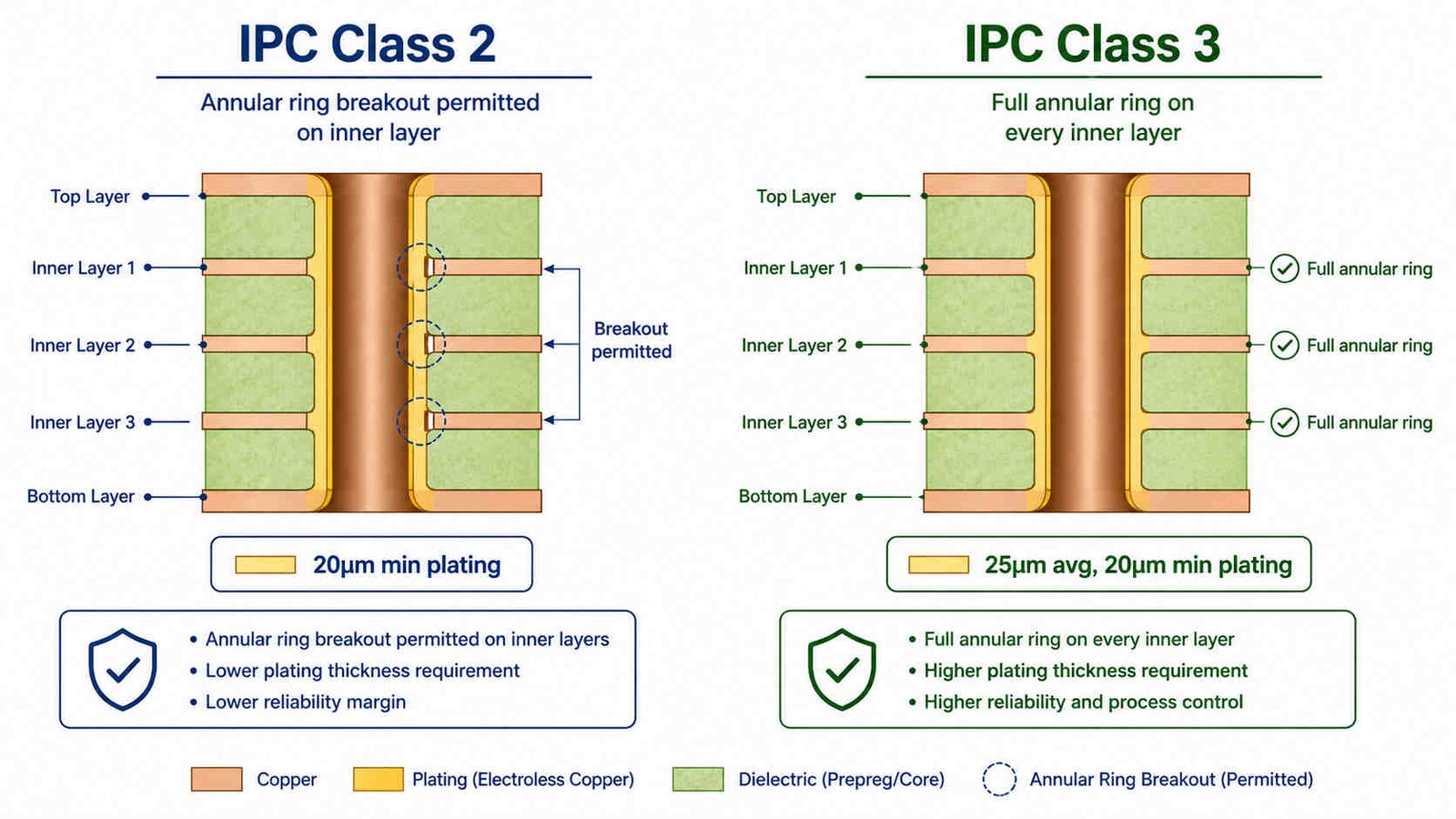
| Requirement | IPC Class 2 | IPC Class 3 |
|---|---|---|
| Annular ring (inner layer) | Breakout permitted | No breakout — confirmed ring required on every layer |
| PTH copper plating | 20 µm average minimum | 25 µm average, 20 µm minimum at any point |
| Void limit per hole | 10% maximum | 5% maximum |
| Solder mask registration | Standard tolerance | Tighter registration control |
| Microsection FAI | On request | Standard requirement |
| Typical application | Commercial, industrial | Aerospace, defense, medical implantable, high-reliability |
IPC Class 3 is the standard specification level for aerospace, defense, and other high-reliability applications where board failure has severe consequences. The core differences from Class 2 are process control requirements, not electrical performance — a Class 2 and Class 3 board with identical stackup and material will have the same Dk, Df, and impedance. What differs is manufacturing tolerance and verification: Class 3 requires no annular ring breakout on any inner layer, thicker minimum copper plating (20µm minimum at any point vs 20µm average for Class 2), and standard microsection first-article inspection.
Specifying IPC Class 3 without confirming your fabricator’s actual process capability for the specific stackup is a common source of yield problems. Dense multilayer designs with fine trace/space may require larger minimum pad sizes to achieve Class 3 annular ring requirements — confirm minimum pad size during DFM review before finalizing layout, not after Gerber submission.
Material Lot Traceability
Aerospace and defense procurement typically requires the ability to trace a finished board back to the specific material lots used in its construction — the CCL lot, copper foil lot, and prepreg lot. This matters for two reasons: it supports anomaly investigation if a field failure occurs (was this a lot-specific issue or a design issue?), and it supports the qualification argument that the material used in production matches the material used in qualification testing.
Request confirmation from your PCB fabricator that they can provide material lot certificates and maintain lot traceability records for your order. This is a process capability question — not every factory maintains lot-level traceability by default, particularly factories optimized for high-volume commercial production where material lots are frequently mixed across orders.
Documentation Checklist for Defense and Aerospace Orders
| Documentation | What It Confirms |
|---|---|
| Material lot Dk/Df certificate | Actual measured Dk/Df for the specific material lot — not nominal datasheet value |
| Copper foil certificate | Foil type, treatment, thickness for the specific production lot |
| Microsection FAI report | Cross-section photo verifying copper plating thickness, void percentage, and annular ring |
| TDR impedance report | Per-panel or per-lot impedance verification at specified tolerance |
| Material lot traceability | Chain of custody from raw material lot to finished board — required for anomaly investigation |
| Certificate of Conformance (C of C) | Formal statement that the board meets specified requirements — commonly required for defense procurement |
| RoHS / REACH declaration | Material compliance documentation — often required regardless of end application |
Environmental Test Considerations
| Test Category | Common Reference | Relevance to PCB Design |
|---|---|---|
| Thermal cycling | MIL-STD-202, IPC-TM-650 | Via barrel and plated hole reliability under repeated temperature swings |
| Vibration / shock | MIL-STD-810 | Mechanical robustness of solder joints and via structures under dynamic load |
| Thermal shock | IPC-TM-650 2.6.7.2 | Rapid temperature transition — more severe than gradual thermal cycling |
| Outgassing (space/vacuum) | ASTM E595 | TML <1.0%, CVCM <0.1% — relevant for satellite and high-altitude applications |
| Humidity resistance | IPC-TM-650 2.6.3 | Moisture ingress resistance — relevant for unsealed or field-deployed electronics |
| Insulation resistance | IPC-TM-650 2.6.3.2 | Dielectric integrity after environmental exposure |
Environmental test requirements vary significantly by application — a ground-based radar system, an airborne avionics box, and a satellite payload have very different thermal, vibration, and vacuum exposure profiles. The PCB fabricator’s role is typically not to perform these tests (they are usually performed at the assembly or system level), but to provide material and process data that supports your qualification argument — Dk/Df stability over temperature, CTE data, and material certificates that confirm the substrate used matches what was qualified.
Material Selection Considerations for Defense RF Applications
Dk stability over temperature
For designs that must maintain electrical performance across a wide operating temperature range (typically -40°C to +85°C or wider for military specifications), Dk thermal coefficient (TCDk) matters. Rogers RO4350B has TCDk of approximately +50 ppm/°C — over a 125°C range, this produces a Dk shift of approximately 0.02, small enough to be negligible for most designs but worth confirming against your specific electrical tolerance budget. See Rogers PCB manufacturer for material datasheets with full temperature coefficient data.
PTFE materials and plasma activation reliability
For defense RF designs using PTFE materials (RO3003, RT5880) that will experience field thermal cycling, in-house plasma activation with controlled timing is critical for long-term via reliability. See PTFE PCB manufacturing challenges for the specific process factors that determine whether a PTFE board survives extended thermal cycling in field deployment.
What to Specify on the Fabrication Drawing
- IPC Class explicitly — ‘2’ or ‘3’ — do not leave this as a default assumption
- Material lot traceability requirement — ‘Provide material lot certificates and maintain traceability records’
- Microsection FAI requirement — ‘First article microsection required, showing copper plating thickness and via structure’
- Impedance tolerance and TDR verification — with specific tolerance and measurement point requirements
- Certificate of Conformance requirement — if required by your end customer’s procurement process
- Any applicable material specification callouts — Dk/Df tolerance, thermal coefficient limits, if relevant to your qualification
Aerospace & Defense PCB Material Qualification — Q&A
Common questions about IPC Class 3 requirements, material traceability documentation, and environmental test standards for aerospace and defense PCB.
What is the difference between IPC Class 2 and Class 3 PCB?
Class 3 requires no annular ring breakout on any inner layer, thicker minimum copper plating (25µm average, 20µm minimum vs 20µm average for Class 2), and standard microsection FAI. Class 3 is standard for aerospace, defense, and other high-reliability applications.
What documentation should I request for a defense PCB order?
Request material lot Dk/Df certificates, copper foil certificates, microsection FAI reports, TDR impedance reports, material lot traceability records, and a Certificate of Conformance if required. Confirm your fabricator maintains lot-level traceability before ordering.
Does IPC Class 3 change the electrical performance of a PCB?
No. IPC Class 3 is a manufacturing process control and verification specification, not electrical performance. A Class 2 and Class 3 board on identical stackup and material have the same Dk, Df, and impedance — Class 3 changes annular ring and plating requirements, improving reliability and consistency.
What test standards apply to aerospace and defense PCB?
Common references include MIL-STD-202 and IPC-TM-650 for thermal cycling, MIL-STD-810 for vibration/shock, ASTM E595 for outgassing, and IPC-TM-650 2.6.3 for humidity/insulation resistance. These are typically performed at assembly/system level — the fabricator provides material data supporting qualification.
IPC Class 3 Available — Material Traceability and Microsection FAI
Rogers RO3003, RT5880, RO4350B in stock with full material lot certificates. IPC Class 2 standard, Class 3 on request. Microsection FAI reports and Certificate of Conformance available. IATF16949 and ISO13485 certified.
Aerospace & Defense PCB → WhatsAppRequest a PCB Quote
Upload your Gerber ZIP file and project requirements. Our engineering team will review your PCB material, stackup, impedance needs, surface finish, and production quantity before quoting.
Please prepare:
- Gerber files in ZIP format
- PCB material or stackup requirements
- Controlled impedance notes if available
- Prototype or batch production quantity