
Blind and Buried Via RF PCB Design — Lamination Cycle Limits and When to Use Each
Blind and buried vias solve the via stub problem by eliminating the unused via barrel entirely, rather than shortening it as backdrill does. But blind via structure in RF PCB is constrained by a factor that is easy to overlook until it becomes a stackup problem: each blind via stage consumes a lamination press cycle, and PTFE materials have a hard limit of 2 cycles total. This guide covers how blind and buried vias work, the lamination cycle constraint that governs how many stages are achievable, and when to specify blind via versus backdrill for a given design.
Home » Blind and Buried Via RF PCB Design — Lamination Cycle Limits and When to Use Each
Table of Contents
How Blind and Buried Vias Are Built
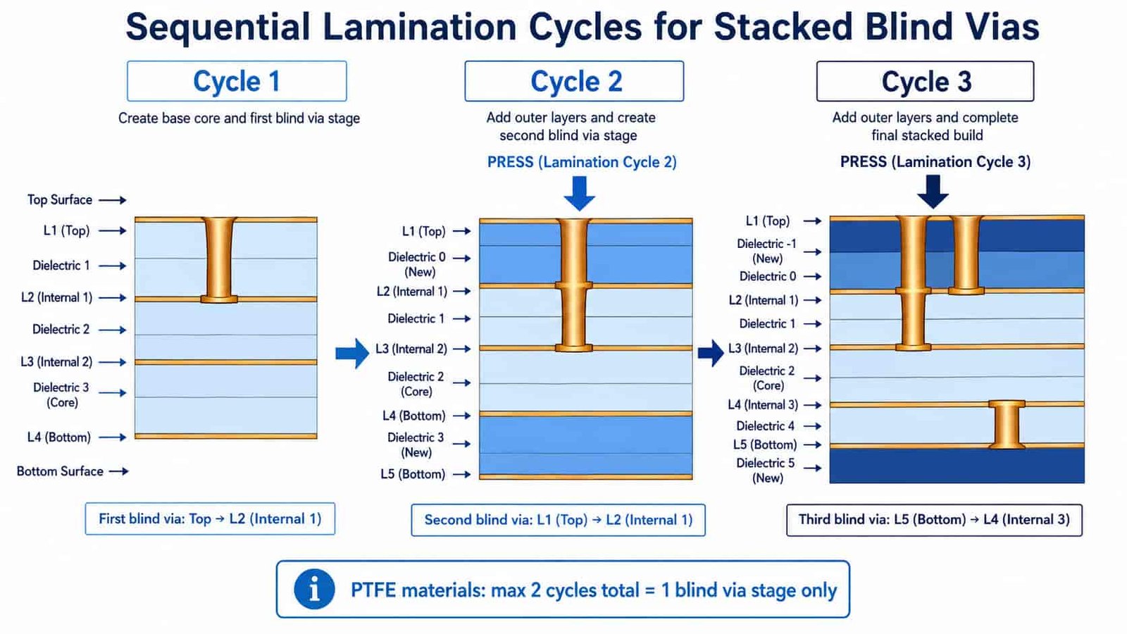
A blind via connects an outer layer to an inner layer without passing through the full board thickness. It is created by drilling and plating a via on a sub-assembly (a subset of the full stackup) before that sub-assembly is laminated to the rest of the board. A buried via connects two or more inner layers without reaching either outer surface — also created on a sub-assembly before final lamination. Each sub-assembly requires its own press cycle, which is why blind and buried via stages are directly tied to the total number of lamination cycles the material can tolerate.
Lamination Cycle Constraints by Material
| Material | Max Lamination Cycles | Achievable Blind Via Stages |
|---|---|---|
| Rogers RO4350B / RO4003C (hydrocarbon) | 3 cycles | 2 blind via stages — e.g. L1-L2 and L(n-1)-Ln |
| Rogers RO3003 / RT5880 (PTFE) | 2 cycles | 1 blind via stage — e.g. L1-L2 only |
| Taconic PTFE grades | 2 cycles | 1 blind via stage — same PTFE constraint |
| F4B PTFE grades | 2 cycles | 1 blind via stage — same PTFE constraint |
| Standard FR4 | Higher cycle tolerance typical | Multiple stages generally feasible — confirm with fabricator |
This constraint is the single most important planning factor for blind via design on PTFE materials. A design that requires 2 blind via stages (for example, L1-L2 on the top side and L(n-1)-Ln on the bottom side) is achievable on RO4350B or RO4003C but not on RO3003 or RT5880 — the PTFE material’s 2-cycle limit only accommodates 1 blind via stage total, consuming both available cycles on the base stackup plus one blind via operation.
If your design requires 2 blind via stages and also needs RF performance only available from a PTFE material (above 20GHz, or Df 0.0010 or lower), the lamination cycle constraint and the material requirement are in direct conflict. Resolve this at the design stage — either reduce to 1 blind via stage, or reconsider whether the RF performance requirement can be met with a hydrocarbon ceramic material (RO4350B/RO4003C) that allows 2 stages.
Blind Via vs Backdrill — Which to Specify
| Requirement | Blind Via | Backdrill |
|---|---|---|
| Via stub elimination completeness | Complete — no stub at all | Partial — ≤10mil stub remaining |
| Additional lamination cycle needed | Yes — consumes a cycle from the material's total limit | No — separate process step after fabrication |
| Cost relative to standard through-hole | Higher — additional press cycle and process complexity | Moderate — extra drilling operation, no added lamination |
| Best for | Fine-pitch, compact modules, Ka-band and above where any stub resonance risk must be eliminated | Backplane connectors, larger via diameter, boards where lamination cycles are already at the material limit |
| PTFE material compatibility | Limited to 1 stage due to 2-cycle max | Compatible regardless of lamination cycle count |
For designs where lamination cycles are already fully consumed by the required stackup (for example, a PTFE hybrid stackup with the material already at its 2-cycle limit for other reasons), backdrill is the only stub-elimination option remaining — it operates on the completed board after final lamination and does not consume an additional press cycle.
Impedance Transition at Blind Via
A blind via presents an impedance discontinuity where the signal transitions from the trace to the via barrel and back to a trace on a different layer. The magnitude of this discontinuity depends on via diameter, pad size (anti-pad), and the length of via barrel relative to the signal wavelength. For microvia-scale blind vias (0.1-0.15mm laser drilled) at frequencies up to Ka-band, this discontinuity is generally small relative to other design tolerances, but for larger-diameter blind vias or designs above 40GHz, EM simulation of the via transition is recommended before finalizing layout.
Buried Via Considerations
Buried vias connecting only internal layers do not appear on either outer surface, which can simplify surface routing density on both outer layers. The tradeoff is that buried vias cannot be inspected visually or by X-ray as easily as through-hole or blind vias, and any defect is only detectable through electrical test or destructive cross-section. For RF designs where via reliability is critical (aerospace, defense applications), confirm your fabricator’s inspection process for buried via structures specifically, not just the general via inspection process.
Stackup Planning Checklist for Blind/Buried Via RF PCB
- Count total lamination cycles required by your stackup — base layers plus each blind/buried via sub-assembly
- Confirm this cycle count against your material’s maximum — 2 for PTFE (RO3003, RT5880, Taconic, F4B), 3 for hydrocarbon ceramic (RO4350B, RO4003C)
- If cycle count exceeds the material limit, resolve during design: reduce blind via stages, or reconsider material selection against RF requirements
- For designs at the cycle limit, evaluate whether backdrillcan substitute for a blind via stage without unacceptable stub resonance
- Specify start/stop layers explicitly for each blind via and buried via on the fabrication drawing and stackup diagram — do not leave this to inference from the Gerber files alone
Blind and Buried Via RF PCB — Q&A
Common questions about lamination cycle limits, blind via vs backdrill, and impedance discontinuity at via transitions.
How many blind via stages can I use with Rogers RO3003 or RT5880?
One blind via stage. PTFE materials have a maximum lamination cycle limit of 2, and each blind via stage consumes one cycle. If your design requires 2 stages, this requires a hydrocarbon ceramic material like RO4350B or RO4003C, which allow 3 lamination cycles.
Should I use blind via or backdrill to eliminate via stub?
Blind via eliminates the stub completely but consumes a lamination cycle — preferred for fine-pitch designs or Ka-band and above. Backdrill leaves a small remaining stub but doesn't consume a cycle — better when your material's cycle budget is already used, or for larger connector vias.
What is the difference between blind via and buried via?
Blind via connects an outer layer to an inner layer without passing through the full board. Buried via connects two or more inner layers without reaching either outer surface. Both are built on a sub-assembly before final lamination and consume a press cycle.
Does a blind via create an impedance discontinuity in RF PCB?
Yes, magnitude depends on via diameter, anti-pad size, and barrel length relative to wavelength. For microvia-scale blind vias up to Ka-band, the discontinuity is generally small. For larger vias or above 40GHz, EM simulation is recommended before finalizing layout.
Blind Via, Buried Via and Backdrill All Supported
Laser microvia to 0.10mm, stackup review confirms lamination cycle feasibility before fabrication starts. Free DFM review checks blind via structure against your material selection.
Free DFM Review → WhatsAppRequest a PCB Quote
Upload your Gerber ZIP file and project requirements. Our engineering team will review your PCB material, stackup, impedance needs, surface finish, and production quantity before quoting.
Please prepare:
- Gerber files in ZIP format
- PCB material or stackup requirements
- Controlled impedance notes if available
- Prototype or batch production quantity