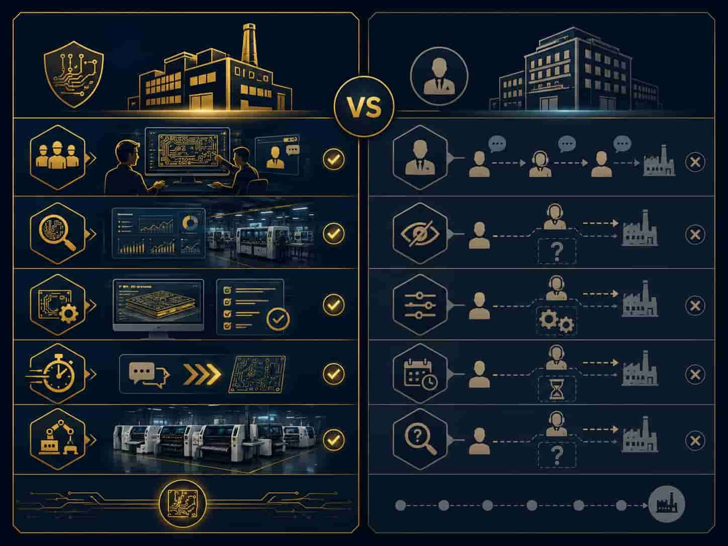
Selecting a high frequency PCB manufacturer is one of the most consequential procurement decisions in an RF or microwave electronics program. The difference between a manufacturer with genuine Rogers and PTFE production capability and one that brokers orders to an unqualified factory can mean the difference between a board that performs to specification and one that fails impedance testing, delaminates, or arrives with plating voids.
High frequency PCB — whether Rogers PCB, PTFE PCB, microwave PCB, or antenna PCB — requires specialized materials, process controls, and equipment that not all PCB factories possess. A factory that produces excellent FR4 commercial PCB may not have the process knowledge, equipment calibration, or material handling experience to produce reliable Rogers or PTFE high frequency boards to IPC Class 3 standards.
This guide covers the capability specifications to verify, the questions to ask, what a genuine DFM engineering review looks like, why working directly with a factory matters, and how to identify manufacturers who genuinely have high frequency PCB production capability versus those who are sourcing through intermediaries.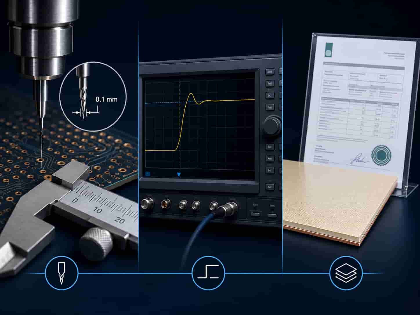
Drilling Capability
Drilling capability for high frequency PCB is more demanding than for standard FR4. Minimum hole diameter, aspect ratio limits, and hole position tolerance all affect via reliability and RF ground performance.
- Minimum mechanical drill diameter: standard 0.2 mm, advanced 0.1 mm — ask which the factory can reliably produce for PTFE materials
- Maximum aspect ratio: standard 10:1, advanced 14:1 — confirm for the specific board thickness and material
- Hole position tolerance: standard ±0.075 mm, advanced ±0.05 mm — critical for fine-pitch via fences and RF connector holes
- Hole diameter tolerance: standard ±0.075 mm, advanced ±0.05 mm
- PTFE-specific parameters: ask whether the factory uses different spindle speed and feed rate for PTFE versus FR4 — a genuine PTFE factory will say yes and be able to describe the parameters
Controlled Impedance Capability
Controlled impedance is a core requirement for high frequency PCB. The factory must have both the process capability to achieve the specified tolerance and the measurement equipment to verify it.
- Standard impedance tolerance: ±10% for traces ≥50Ω — every qualified high frequency factory should achieve this
- Advanced impedance tolerance: ±8% — ask whether the factory can achieve this and under what conditions
- Below 50Ω absolute tolerance: ±5Ω standard, ±3.5Ω advanced — ask for evidence from recent production
- TDR measurement equipment: factory should have its own TDR — not send coupons to an external lab
- Coupon design: ask to see a sample impedance coupon design — a factory with genuine impedance capability has a standard coupon layout
- Measurement frequency: TDR measurement at what frequency? Ask for actual measurement records from recent jobs
PTFE and Rogers Material Processing
Processing Rogers and PTFE materials requires specific equipment, chemicals, and process knowledge that FR4-only factories do not have. These are the most revealing questions to ask a potential high frequency PCB supplier.
- Hole wall activation: does the factory use sodium naphthalene (wet chemical) or plasma activation for PTFE? Can it describe the process? Both are valid — the factory should know which it uses
- Rogers bonding film inventory: does the factory stock Rogers RO4450F, RO4450T, or Rogers 2929 bondply? Ask which bonding films are in inventory
- PTFE lamination parameters: does the factory use different press temperature and pressure profiles for PTFE versus FR4? It should
- Drill entry and exit material: does the factory use PTFE-specific cover and backer materials for drilling thin PTFE substrates? Ask
- Maximum lamination cycles: can the factory confirm the 2-cycle limit for PTFE and 3-cycle limit for Rogers hydrocarbon? A knowledgeable factory will confirm this without hesitation
Layer Count and Stackup Capability
- Standard layer count: 2–32 layers — most high frequency factories support this range
- Advanced layer count: up to 50 layers — ask if needed for high-density designs
- Minimum board thickness by layer count: 0.2 mm for 2 layers, 0.36 mm for 4 layers, 0.575 mm for 6 layers — a factory should know these limits
- Minimum dielectric thickness: 0.065 mm (1080H prepreg) standard, 0.05 mm (106H) advanced — verify for thin-layer Ka-band designs
- HDI capability: 1–3 stages standard, 1–6 stages advanced — ask for PTFE-compatible HDI process specifically
Copper Plating Capability
- PTH copper plating thickness: ≥20 µm standard, 20–50 µm range — ask for IPC Class 3 25 µm average capability
- Blind via fill: convex ≤50 µm, concave ≤76 µm advanced — verify for copper-filled via designs
- Plating bath control: does the factory monitor plating bath chemistry continuously? Ask about replenishment logging
- Microsection capability: does the factory have an in-house metallographic lab for via cross-sections? Ask for a sample microsection photograph
What a Genuine DFM Engineering Review Looks Like
Design for Manufacturability (DFM) review is the pre-production engineering check that identifies issues in the design before production begins. A genuine factory DFM review for high frequency PCB covers specific parameters that standard PCB DFM does not address.
What Should Be Reviewed in High Frequency PCB DFM
- Stackup feasibility: can the specified layer count, dielectric thickness, and copper weight be achieved with the specified material?
- Impedance calculation verification: does the factory re-calculate impedance using its confirmed production Dk values — not nominal datasheet values?
- Bonding film Dk impact: for hybrid Rogers + FR4 stackups, does the factory account for the bonding film Dk in the impedance calculation?
- Via aspect ratio check: does any via in the design exceed the factory’s confirmed aspect ratio limit for the specified material?
- Minimum annular ring verification: are all internal layer pads large enough to guarantee no breakout after drilling position tolerance?
- PTFE process compatibility: if PTFE is included, does the via structure (blind via stages, layer count) fall within the 2-cycle lamination limit?
- Impedance coupon placement: does the factory specify where impedance coupons will be placed on the panel edge?
- Line width vs copper weight: are all trace widths consistent with the minimum line width for the specified copper weight on each layer?
How Long Should DFM Take?
A thorough DFM review for a complex high frequency PCB with Rogers material, controlled impedance, and hybrid stackup takes 1–2 business days for a factory engineering team. Simpler designs may be reviewed within 4 hours.
If a supplier provides a DFM sign-off within minutes of receiving the files without any questions or feedback, one of two things is true: the design is extremely straightforward, or no genuine DFM review was performed. For complex high frequency designs, the latter is more likely.
What DFM Feedback Should Look Like
A genuine DFM review produces specific, technical feedback. Examples of real DFM comments from an experienced high frequency factory:
- ‘The via aspect ratio on your blind vias in the PTFE layers reaches 0.95:1, which exceeds our 0.9:1 advanced capability limit. We recommend reducing the PTFE substrate thickness from 0.254 mm to 0.127 mm or increasing the laser via diameter from 3 mil to 4 mil.’
- ‘Layer 3 to Layer 4 impedance calculation uses Dk 3.0 (RO3003 nominal) but our production Dk for this lot is 3.02. Recalculating gives 49.3Ω — within ±10% tolerance. No change required.’
- ‘The internal layer 3 pad for via V12 has a 0.3 mm pad diameter. After drilling with ±0.05 mm position tolerance, the minimum annular ring is 0.025 mm — at the IPC Class 3 limit. We recommend increasing the pad to 0.35 mm for margin.’
This level of specific, quantitative DFM feedback is only possible from an engineering team that is directly involved in production. For stackup planning background, see RF PCB Stackup Design: Key Factors Before Manufacturing.
Riching PCB Manufacturing Capability — Direct Factory Specifications
As a direct high frequency PCB manufacturer, we produce Rogers, PTFE, Taconic, F4B, and hybrid high frequency PCB in our own factory. The following specifications represent our confirmed production capability — not claimed capability from a third party.
Drilling
- Minimum mechanical drill diameter: 0.1 mm advanced capability, 0.2 mm standard
- Maximum aspect ratio: 14:1 advanced, 10:1 standard
- Hole diameter tolerance: ±0.05 mm advanced, ±0.075 mm standard
- Hole position tolerance: ±0.05 mm advanced, ±0.075 mm standard
- PTFE drilling: dedicated parameters for Rogers RT5880, RO3003, Taconic, F4B materials
Controlled Impedance
- Standard tolerance: ±10% for traces ≥50Ω, ±5Ω for traces <50Ω
- Advanced tolerance: ±8% for traces ≥50Ω, ±3.5Ω for traces <50Ω
- Impedance verification: in-house TDR measurement, coupon on every production lot
- Calculation method: confirmed production Dk from material certificate — not nominal values
Layer Count and Stackup
- Standard layer count: 2–32 layers
- Advanced layer count: up to 50 layers
- Minimum board thickness: 2L = 0.2 mm, 4L = 0.36 mm, 6L = 0.575 mm
- Minimum dielectric: 0.065 mm (1080H), 0.05 mm (106H) advanced
- HDI: 1–6 stages advanced, PTFE-compatible laser blind via process
- Lamination cycles: maximum 3 for FR4/Rogers hydrocarbon, maximum 2 for PTFE
Copper Plating
- PTH copper plating: 20–50 µm range, IPC Class 3 25 µm average capability
- Blind via fill: convex ≤50 µm, concave ≤76 µm advanced
- Microsection: in-house metallographic lab, FAI microsection standard
Line Width and Spacing
- Outer layer: 2.5 mil / 3 mil advanced, 3 mil / 4 mil standard
- Inner layer: 2.7 mil / 2.7 mil advanced, 3 mil / 3 mil standard
- Etching tolerance: ±1 mil for traces <10 mil, ±10% for impedance traces ≥10 mil
Materials in Production
- Rogers: RO4350B, RO4003C, RO3003, RO3003G2, RT5880, RT5870, RO3006, RO3010, RO6010
- Taconic: TLY-5, TLY-5A, TLP-5, TLY-3, RF-35, RF-60A, CER-10
- F4B (旺灵): F4BM220, F4BM255, F4BM265, F4BM300, F4BTM400, F4BTM440, F4BTM615
- ZY (中英): ZYF220D, ZYF225DA, ZYF265D, ZYF300CA-P, ZYF350CA
- FR4 hybrid: full hybrid capability with all Rogers and PTFE materials above
For material specifications and properties, see Rogers PCB Material Selection Guide for RF and Microwave Applications, Taconic PCB Materials for RF and Microwave Applications, and F4B PCB Material Guide.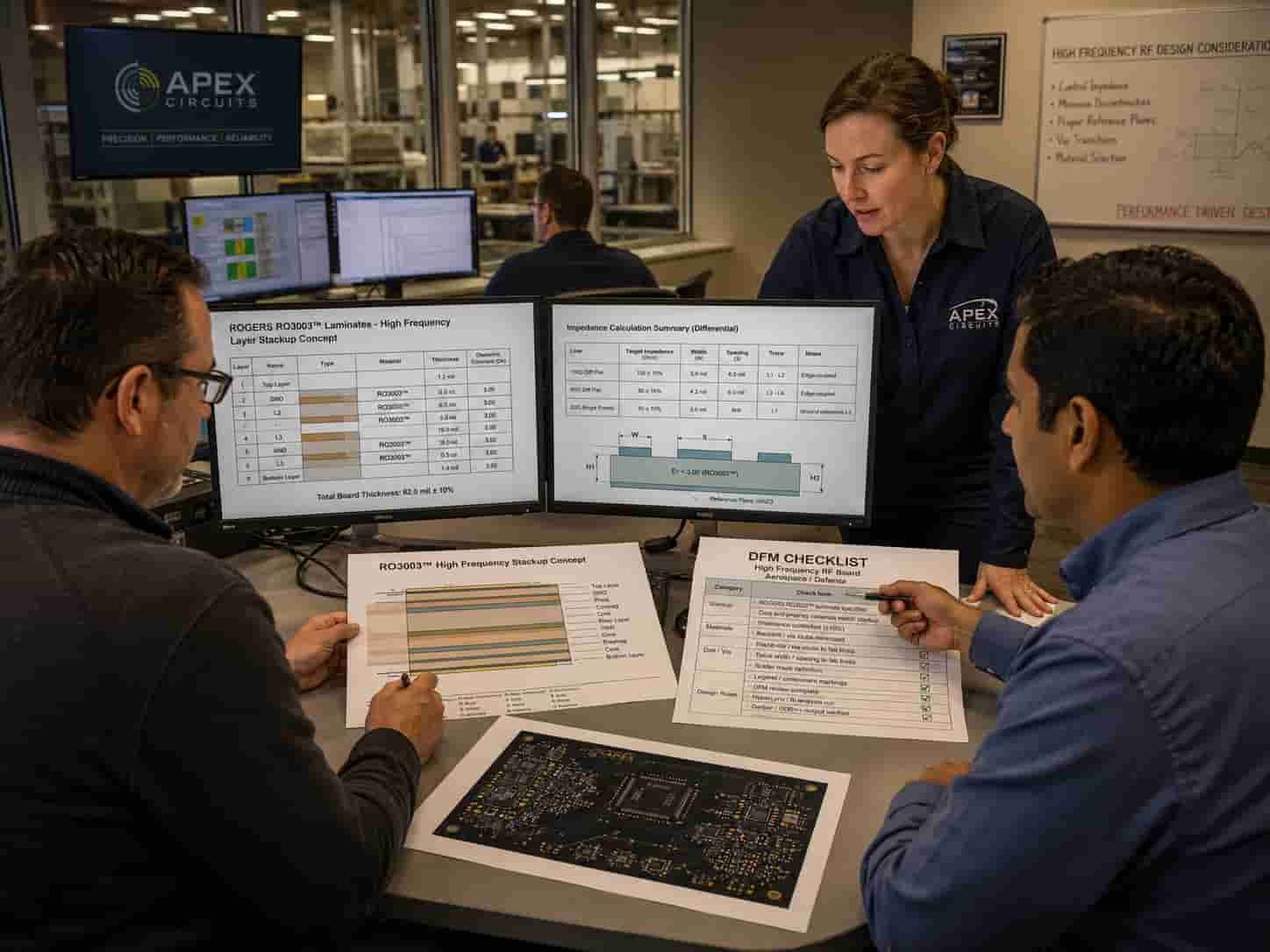
Questions to Ask Before Placing a High Frequency PCB Order
The following questions help verify whether a potential high frequency PCB supplier has genuine production capability or is acting as an intermediary. A direct factory with real capability will answer these questions specifically and quickly.
Process Questions
- ‘What PTFE hole wall activation method do you use — sodium naphthalene or plasma? Can you describe the process sequence?’
- ‘Which Rogers bonding film do you use for RO4350B-to-FR4 hybrid stackups? Do you stock RO4450F?’
- ‘What is your confirmed minimum drill diameter for Rogers RT5880 at 0.254 mm thickness?’
- ‘Can you provide a sample TDR impedance measurement record from a recent production lot?’
- ‘What is your maximum lamination cycle count for a pure PTFE stackup?’
- ‘Do you perform impedance calculation using nominal Dk or confirmed production Dk from the material certificate?’
Quality Questions
- ‘Do you have an in-house metallographic lab for microsection analysis, or do you send samples to an external lab?’
- ‘Can you provide a sample microsection photograph from a recent IPC Class 3 high frequency PCB?’
- ‘What is your 100% electrical test coverage — all nets, or selected nets?’
- ‘Can you provide material certificates with Rogers Corporation lot numbers for Rogers RO3003?’
- ‘What is your process for impedance coupon measurement — TDR brand, measurement frequency, coupon design?’
Engineering Questions
- ‘If I send you my Gerber files and stackup, how long will your DFM review take, and what format will the feedback be in?’
- ‘If my design has an aspect ratio that exceeds your standard capability, will you flag it before production or discover it during?’
- ‘Can your engineering team calculate the impedance for my specific stackup using your production Dk values before I finalize the design?’
How We Handle High Frequency PCB Quotation — Direct Factory Process
At Riching PCB, quotation for high frequency PCB follows a direct factory engineering review process. When you submit files, our RF PCB engineering team reviews the design — not a sales team — before quotation is confirmed.
What We Review Before Quoting
- Stackup feasibility: layer count, material compatibility, dielectric thickness, lamination cycle count
- Impedance calculation: we recalculate using our confirmed production Dk for the specified material lot
- Via aspect ratio: every via checked against our confirmed capability for the specified material
- PTFE process compatibility: hole wall activation process confirmed for the specific PTFE material
- Line width vs copper weight: every layer checked for minimum line width compliance
- Bonding film selection: for hybrid stackups, appropriate bonding film confirmed in inventory
- Lead time: production schedule confirmed based on actual factory capacity, not optimistic estimates
What You Receive With Your Quote
- Confirmed stackup with production Dk values used for impedance calculation
- DFM feedback on any issues that require design changes before production
- Confirmed impedance tolerance achievable for the specific design
- Material availability confirmation — Rogers, Taconic, F4B, or ZY as specified
- Lead time based on actual factory schedule
- Impedance coupon design recommendation for the specific layer structure
To submit files for engineering review and quotation, see What Files Are Needed for a High Frequency PCB Quotation?.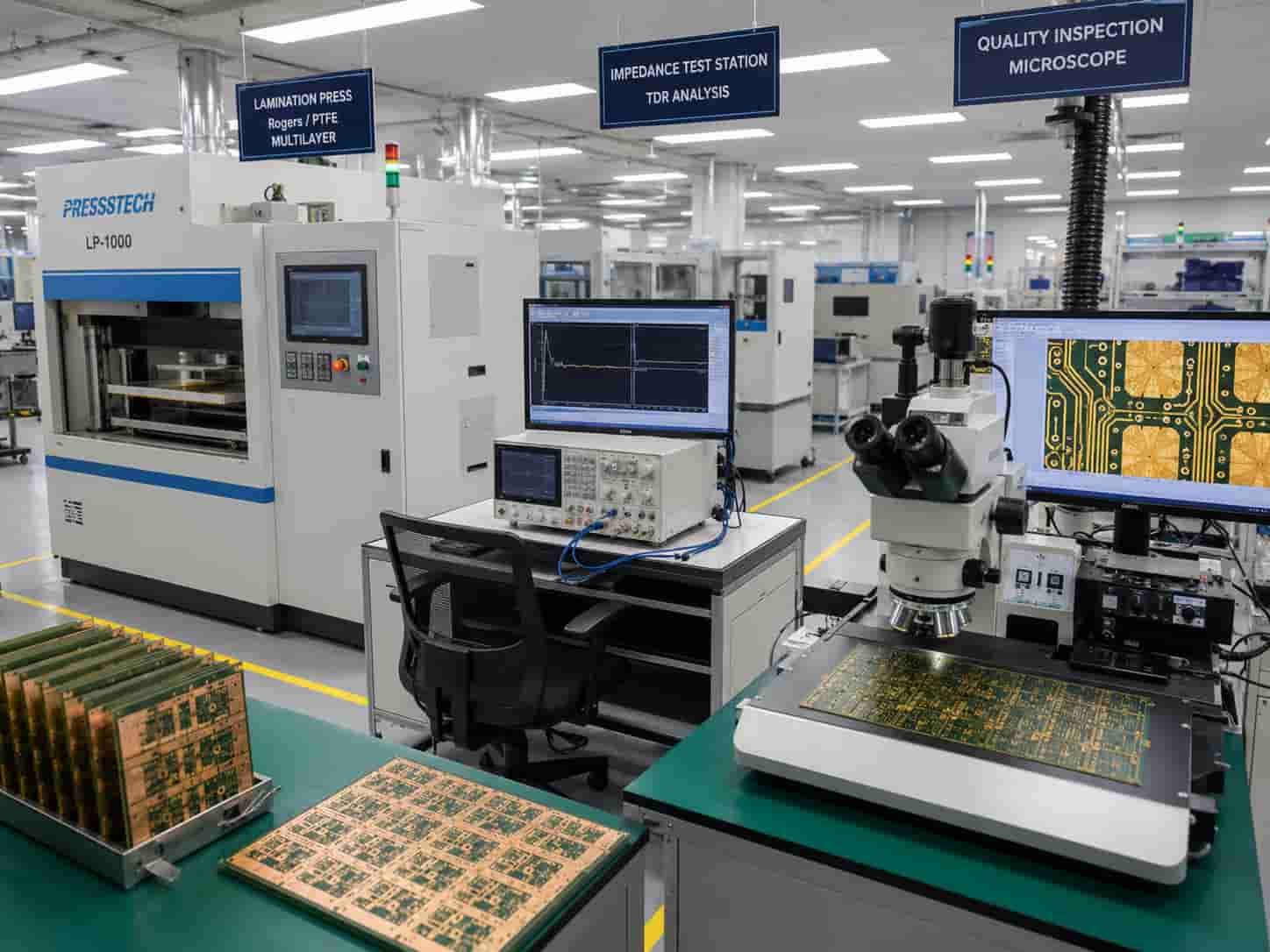
Conclusion
Evaluating a high frequency PCB manufacturer requires going beyond website claims and pricing. The specific process questions about PTFE activation, bonding film selection, impedance coupon design, and microsection capability are reliable indicators of whether a factory has genuine Rogers and PTFE production experience or is sourcing through intermediaries.
A direct factory with real high frequency PCB production capability will answer process questions specifically, provide DFM feedback that is quantitative and technical, produce material certificates with laminate lot traceability, and be able to investigate and resolve production issues directly — not through an intermediary chain. For RF PCB, Rogers PCB, and PTFE PCB projects where first-pass success matters, working directly with a factory that has genuine high frequency production capability is the most reliable path to consistent results.