Electronic Warfare PCB: Materials, EW Band Guide and Manufacturing Requirements
Substrate selection, wideband design considerations and IPC Class 3 manufacturing requirements for ESM, ECM and DRFM electronic warfare PCB.
Home » Defense PCB » Electronic Warfare PCB: Materials, EW Band Guide and Manufacturing Requirements
Table of Contents
Key point: Key point: Most factories quote 3–4 weeks waiting for RO3003 / RT5880 material procurement. Riching PCB maintains these materials in stock — no material wait.
Rogers RO3003 is a PTFE ceramic substrate with Dk 3.0 and Df 0.0010 — standard for Ka-band (26.5–40 GHz), 77 GHz automotive radar and 5G mmWave 28 GHz phased arrays. At 30 GHz, RO3003 insertion loss is ~0.5 dB/cm vs ~1.8 dB/cm for RO4350B. 50Ω microstrip on 0.127 mm RO3003 with 0.5 oz copper: ~0.28 mm trace width. Available thicknesses: 0.127 / 0.254 / 0.508 / 0.762 / 1.524 mm. All RO3003 orders require in-house plasma hole wall activation and maximum 2 lamination press cycles. Riching PCB stocks RO3003 in 0.127 mm and 0.254 mm with in-house plasma activation. No MOQ. Prototype 7–10 working days.Electronic warfare PCB for wideband ESM and ECM systems (2–18 GHz) requires Rogers RT5880 (Dk 2.20, Df 0.0009) — the lowest-loss, most Dk-stable PTFE substrate across a decade of bandwidth. Narrowband EW below 12 GHz can use RO3003 (Df 0.0010). All PTFE materials require in-house plasma hole wall activation. Defense EW PCB requires IPC Class 3 manufacturing, TDR impedance verification to ±5% on every production lot, and maximum 2 PTFE lamination press cycles. Riching PCB stocks RT5880 and RO3003 with in-house plasma activation. No MOQ. Prototype lead time 7–10 working days.
Electronic warfare PCB covers one of the most demanding RF design categories — wideband receivers and jammers operating from 2 GHz to 18 GHz or beyond, requiring consistent low-loss performance across a decade or more of bandwidth. A single substrate material must maintain stable Dk and minimum Df across the entire operating band, survive thermal and mechanical shock in airborne or shipborne environments, and meet IPC Class 3 reliability requirements for defense applications.
This guide covers EW frequency bands and their PCB material requirements, why RT5880 is the standard for wideband EW systems, manufacturing requirements for defense-grade EW PCB, and what to specify when ordering from a fabricator.
EW Frequency Bands and Material Selection
| EW Band | Frequency Range | Typical Function | Recommended Material |
|---|---|---|---|
| VHF/UHF | 30 MHz–3 GHz | Communications EW, jamming | RO4350B or FR4 hybrid |
| S-band | 2–4 GHz | Radar warning, ESM | RO4350B |
| C-band | 4–8 GHz | ESM, jamming | RO4350B or RT5880 |
| X-band | 8–12 GHz | Radar warning, jamming, DRFM | RT5880 or RO3003 |
| Ku-band | 12–18 GHz | EW receiver, jammer | RT5880 |
| K/Ka-band | 18–40 GHz | Wideband EW, mmWave EW | RT5880 or RO3003 |
| Wideband 2–18 GHz | 2–18 GHz | Wideband ESM/ECM systems | RT5880 (entire band) |
The key challenge in EW PCB design is wideband coverage. A radar warning receiver (RWR) or electronic support measures (ESM) system must cover 2–18 GHz with a single antenna and RF front-end. This rules out material choices optimized for a single frequency — Dk and Df must remain consistent across the entire band.
Why RT5880 Is the Standard for Wideband EW PCB
Rogers RT5880 (Dk 2.20, Df 0.0009) is the standard substrate for wideband EW systems covering 2–18 GHz for three reasons:
- Lowest Df of any standard Rogers material (0.0009) — consistent insertion loss from 2 GHz to 18 GHz and beyond
- Lowest Dk variation with frequency — Dk remains within ±0.02 from 1 GHz to 40 GHz, critical for wideband antenna and filter design
- Lowest Dk variation with temperature — critical for airborne EW systems operating from –55°C to +125°C
RT5870 (Dk 2.33, Df 0.0012) is the alternative when a slightly higher Dk is required for more compact circuit dimensions. Both RT5880 and RT5870 use the same PTFE glass construction and require the same plasma activation process.
For narrowband EW applications at a fixed frequency below 12 GHz, Rogers RO3003 (Df 0.0010) is a cost-effective alternative. See Rogers materials overview for full thickness and Dk/Df specifications.
Material Selection for EW PCB
| Material | Dk | Df | Type | EW Suitability |
|---|---|---|---|---|
| RT5880 | 2.20 | 0.0009 | PTFE glass | ✅ Best — lowest loss, wideband 2–18 GHz and beyond |
| RT5870 | 2.33 | 0.0012 | PTFE glass | ✅ Good — slightly higher Dk, same process as RT5880 |
| RO3003 | 3.0 | 0.0010 | PTFE ceramic | ✅ Good — suitable for narrowband EW below 12 GHz |
| Taconic TLY-5 | 2.17 | 0.0009 | PTFE glass | ✅ Suitable — similar to RT5880 |
| RO4350B | 3.48 | 0.0037 | Hydrocarbon | ⚠️ Lower bands only — acceptable below 6 GHz |
| Standard FR4 | ~4.5 | ~0.020 | Epoxy glass | ❌ Not suitable — excessive loss above 3 GHz |
Manufacturing Requirements for Defense EW PCB
IPC Class 3 Compliance
Defense EW PCB requires IPC Class 3 manufacturing — the highest reliability class, covering hole wall copper thickness (minimum 25 µm), annular ring requirements, solder mask coverage, and dimensional tolerances. IPC Class 3 applies to airborne, shipborne, and ground vehicle EW systems where field repair is not possible. Specify IPC Class 3 explicitly on the fabrication drawing and verify your fabricator’s certification before placing an order.
PTFE Plasma Activation
RT5880, RT5870, RO3003, Taconic TLY-5, and all F4B PTFE materials require in-house plasma hole wall activation before copper plating. For defense EW PCB, this process must be performed in-house — outsourcing plasma activation introduces process control risk that is unacceptable for IPC Class 3 applications. See PTFE PCB manufacturing challenges for full process detail.
Impedance Control
Wideband EW PCB requires impedance control to ±5% across the operating band, verified by TDR on every production lot. For DRFM (Digital Radio Frequency Memory) and wideband receiver designs, impedance discontinuities at connectors, via transitions, and trace width changes must be minimized. Specify impedance tolerance and TDR verification on the fabrication drawing.
Copper Foil
RT5880 and RT5870 are available with standard electrodeposited (ED) copper foil for most EW applications. For designs operating above 18 GHz or where insertion loss budget is critical, low-profile (LP) copper foil reduces surface roughness contribution. Specify copper foil type on the stackup drawing — standard ED foil is default unless low-profile is requested.
Surface Finish
ENIG (immersion gold) is the standard surface finish for EW PCB — flat, consistent, and solderable. For defense applications requiring gold thickness above 5 µin, hard gold (electroplated) is available. Immersion silver is not recommended for defense applications due to tarnish sensitivity in humid environments.
Lamination Limit
RT5880, RT5870, and all PTFE materials are limited to a maximum of 2 lamination press cycles. Multi-layer EW PCB requiring more press cycles must use hybrid stackup design with PTFE on outer signal layers and FR4 on inner layers. Consult your fabricator on bondply selection before finalizing the stackup.
Wideband Stackup Design for EW PCB
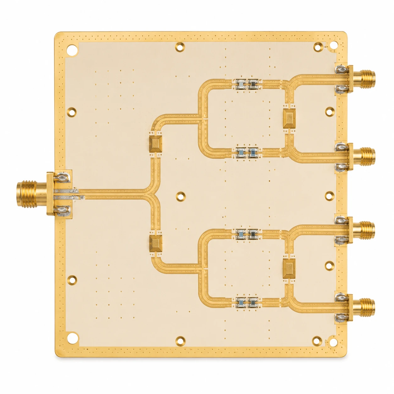
Most wideband EW receiver and jammer PCB uses a 2-layer or 4-layer configuration:
2-Layer RT5880 (ESM receiver front-end)
- Top copper: 1 oz (35 µm) finished
- RT5880 core: 0.254 mm or 0.508 mm
- Bottom copper: 1 oz (35 µm) ground plane
For 50Ω microstrip on 0.254 mm RT5880 with 1 oz copper: trace width approximately 0.74 mm. Lower Dk than RO3003 means wider traces — easier to manufacture at minimum line width.
4-Layer Hybrid (RT5880 + FR4 for mixed EW/digital)
- L1 — RT5880 0.254 mm — wideband RF signal layer
- L2 — Ground plane
- FR4 prepreg — digital processing layers
- L3 — Power/digital signal layer
- FR4 prepreg
- L4 — RT5880 0.254 mm — RF output layer
For DRFM and EW processing systems combining wideband RF with high-speed digital, this hybrid stackup places RT5880 on RF signal layers while using FR4 for digital processing layers. See FR4 + Rogers hybrid PCB stackup guide for bondply selection.
Applications
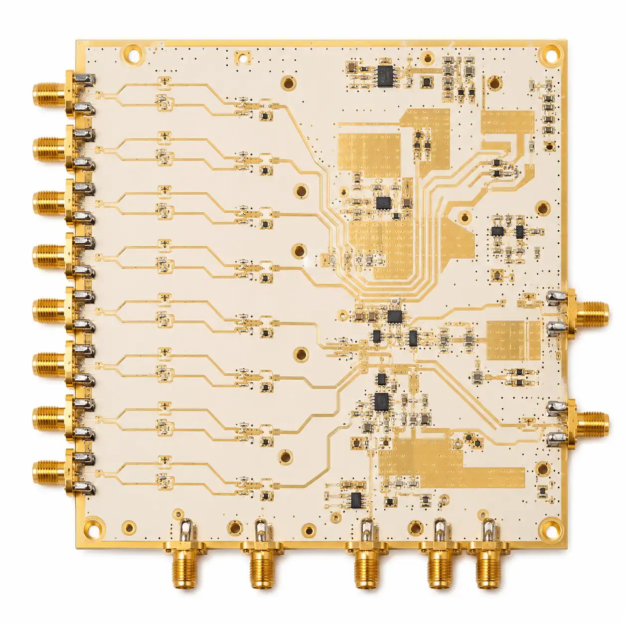
- Radar Warning Receivers (RWR) — airborne, shipborne, ground vehicle
- Electronic Support Measures (ESM) — wideband signal intercept and analysis
- Electronic Countermeasures (ECM) — noise and deception jammers
- Digital Radio Frequency Memory (DRFM) — wideband signal replay and jamming
- Self-Protection Jammer (SPJ) — airborne pod-mounted jamming systems
- Electronic Intelligence (ELINT) — signal collection and analysis systems
- Counter-UAS RF systems — wideband drone detection and jamming
Conclusion
Electronic warfare PCB requires wideband PTFE substrate — Rogers RT5880 (Df 0.0009) is the standard for 2–18 GHz ESM and ECM systems. IPC Class 3 manufacturing, in-house plasma activation, TDR impedance verification to ±5%, and a maximum of 2 PTFE lamination cycles are non-negotiable requirements. Riching PCB manufactures EW PCB with RT5880 and RO3003 in stock, in-house plasma activation, IPC Class 3 capability, no MOQ, and prototype lead time of 7–10 working days. See high frequency PCB capabilities for full factory specifications.
Get a Quote for Your EW PCB
Riching PCB stocks RT5880 and RO3003 with in-house plasma activation. IPC Class 3 available. Send the following for DFM review:
- Gerber files + NC drill file
- Operating frequency range and EW function (ESM / ECM / DRFM)
- Material grade (RT5880 / RT5870 / RO3003) and dielectric thickness
- Stackup drawing — copper weight per layer
- Controlled impedance target and tolerance
- IPC Class (2 or 3) and quantity
WhatsApp +86 13760473650 — DFM review within 24 hours
Electronic Warfare PCB Q&A
Common questions about EW PCB including material selection, RT5880 vs RO4350B, IPC Class 3, impedance requirements and prototype lead times.
What material is used for electronic warfare PCB?
Rogers RT5880 (Dk 2.20, Df 0.0009) is standard for wideband EW covering 2–18 GHz. Lowest Df, stable Dk across frequency and temperature from 2 GHz to 40 GHz — essential for flat frequency response in ESM, ECM, and DRFM systems. For narrowband EW below 12 GHz, RO3003 (Df 0.0010) is a cost-effective alternative.
Why is RT5880 preferred over RO4350B for EW PCB?
RO4350B (Df 0.0037) is acceptable below 6 GHz but produces unacceptable insertion loss at X-band and above. A wideband 2–18 GHz EW receiver cannot use RO4350B — loss varies significantly across the band. RT5880 (Df 0.0009) maintains consistent low loss from 2 GHz to 18 GHz, essential for wideband ESM and ECM systems.
Does electronic warfare PCB require IPC Class 3?
Yes — defense EW PCB requires IPC Class 3 (minimum 25 µm hole wall copper, annular ring and dimensional tolerances). Applies to airborne, shipborne, and ground vehicle systems where field repair is not possible. Specify IPC Class 3 on the fabrication drawing and verify fabricator certification before ordering.
What impedance tolerance is required for wideband EW PCB?
±5% across the operating band, verified by TDR on every production lot. Impedance discontinuities at connectors, via transitions, and trace width changes must be minimized. Trace width calculated from confirmed production Dk — not nominal datasheet values.
What is the lead time for EW PCB prototype?
7–10 working days for RT5880 and RO3003 PTFE. IPC Class 3 available — confirm at order. No MOQ — from 1 board. DFM review before every order. WhatsApp: +86 13760473650.
Request a PCB Quote
Upload your Gerber ZIP file and project requirements. Our engineering team will review your PCB material, stackup, impedance needs, surface finish, and production quantity before quoting.
Please prepare:
- Gerber files in ZIP format
- PCB material or stackup requirements
- Controlled impedance notes if available
- Prototype or batch production quantity
