
High Frequency PCB Drilling Capabilities — Minimum Hole Size, Aspect Ratio and Tolerances
Drilling capability determines what via structures, connector footprints and mechanical features are achievable on a given board thickness and material. This reference covers minimum drill diameter, hole tolerance, aspect ratio limits, and special drilling processes (backdrill, blind via, countersink, half-hole) for high frequency PCB — including the additional process considerations that apply to Rogers and PTFE materials.
Home » High Frequency PCB Drilling Capabilities — Minimum Hole Size, Aspect Ratio and Tolerances
Table of Contents
Standard Drilling Capability
| Parameter | Standard Capability | Advanced Capability |
|---|---|---|
| Minimum drill diameter (mechanical) | 0.20 mm | 0.10 mm (laser) |
| Hole diameter tolerance (PTH) | ±0.075–0.08 mm | ±0.05 mm |
| Hole diameter tolerance (NPTH) | ±0.075–0.08 mm | ±0.05 mm |
| Hole position tolerance | ±0.075 mm | ±0.05 mm |
| Maximum aspect ratio | 10:1 | 14:1 (extreme 15:1 — requires evaluation) |
| Hole-to-hole clearance (same net) | ≥6 mil | — |
| Hole-to-hole clearance (different net) | ≥10 mil | — |
| Maximum board thickness (mechanical drill) | 5.4 mm | — |
| Laser drill hole diameter range | 0.15–6.50 mm (larger holes routed) | — |
These values apply to standard FR4 and Rogers hydrocarbon ceramic materials (RO4350B, RO4003C). PTFE materials (RO3003, RT5880) use the same drill diameter and tolerance limits but require lower spindle speed (40,000–60,000 RPM vs standard FR4 speeds) and PTFE-specific drill bit geometry to avoid hole wall smear — see PTFE PCB manufacturing challenges for detail.
Standard Drilling Capability
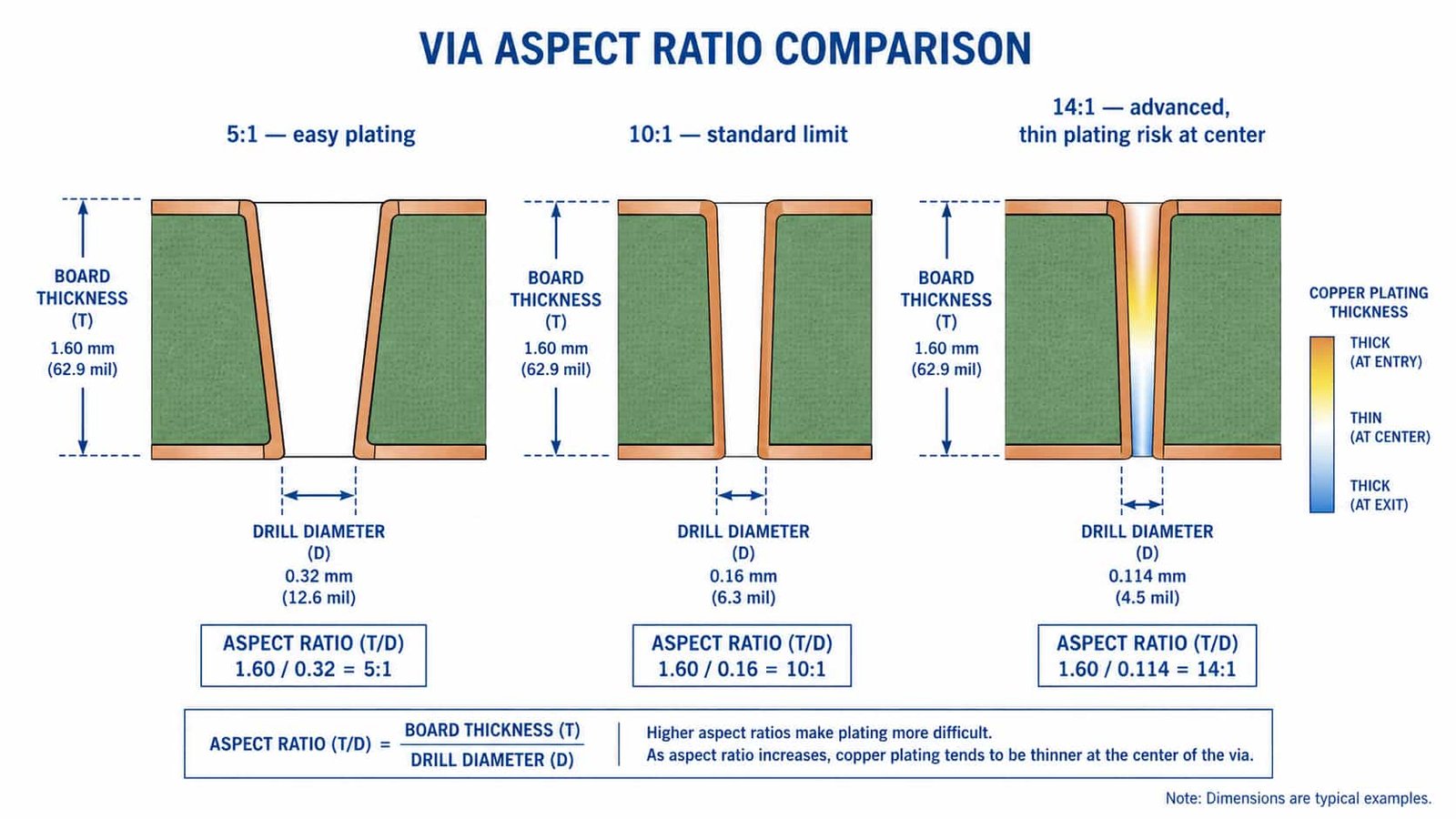
| Board Thickness | Min Drill (10:1 standard) | Min Drill (14:1 advanced) |
|---|---|---|
| 1.0mm | 0.10mm | 0.07mm — below standard minimum, confirm feasibility |
| 1.6mm | 0.16mm | 0.11mm |
| 2.0mm | 0.20mm | 0.14mm |
| 3.0mm | 0.30mm | 0.21mm |
| 4.0mm | 0.40mm | 0.29mm |
| 5.4mm (max mechanical) | 0.54mm | 0.39mm |
Aspect ratio is the ratio of board thickness to via drill diameter. As this ratio increases, the electroplating solution has increasing difficulty reaching the center of the hole barrel uniformly, producing thinner plating at the barrel center relative to the ends. Vias with excessive aspect ratio have a higher risk of thin-plating-related failure under thermal cycling. The 10:1 standard limit and 14:1 advanced limit reflect the point at which reliable, uniform plating becomes progressively more difficult to guarantee.
For thick boards (above 3mm) combined with small via diameters, confirm aspect ratio feasibility with your fabricator before finalizing via sizes in your design — do not assume standard drill sizes will scale linearly to thick multilayer stackups without process risk.
Hole Position and Diameter Tolerance
Hole position tolerance (±0.05mm advanced, ±0.075mm standard) determines how much a drilled hole can deviate from its intended coordinate — this directly affects annular ring reliability, since a hole drilled off-position toward one edge of its pad reduces the copper ring on the opposite side. For designs specifying IPC Class 3 (no annular ring breakout on inner layers), the combination of hole position tolerance and pad size must be checked together — a pad sized for nominal position may violate Class 3 requirements at worst-case position tolerance.
Special Drilling Processes
| Special Process | Capability | Application |
|---|---|---|
| Backdrill | ≤10 mil stub remaining, ±0.1mm depth tolerance | Via stub resonance elimination above 5–15GHz |
| Blind via | 1 stage (PTFE), 2 stages (RO4350B/RO4003C) | HDI, fine-pitch stub-free transitions |
| Buried via | Confirm with fabricator per stackup | Internal layer interconnect without surface impact |
| Countersink / counterbore | 45°/60°/82°/90°/100°, common angle 90° | Connector mounting, mechanical fastening |
| Controlled depth drill | 0.5mm ≤ drill diameter ≤ 1.8mm range | Partial-depth features, stepped cavities |
| Half-hole / castellated hole | 0.4–6.35mm range | Module edge-mount connections, SMD modules |
| Via-in-pad | Resin or copper filled, per IPC-4761 | BGA/QFN direct via placement, thermal via under MMIC |
Backdrill
Backdrilling removes the unused via stub from the back side of a through-hole via to a controlled depth, leaving ≤10 mil remaining stub. This is a separate drilling operation from the standard NC drill file and requires its own file specifying coordinates, diameter, depth and side. See back drill PCB guide for stub resonance frequency calculations and when backdrill is required.
Blind and buried via
Blind vias connect an outer layer to an inner layer without passing through the full board thickness — eliminating via stub entirely rather than shortening it as backdrill does. The number of achievable blind via stages is constrained by lamination cycle limits: PTFE materials allow 1 blind via stage (2 total lamination cycles), while RO4350B and RO4003C allow 2 stages (3 total cycles). Buried vias connect internal layers without reaching either outer surface — feasibility depends on the specific stackup and should be confirmed with the fabricator during DFM review.
Half-hole (castellated edge)
Half-holes — plated holes drilled along the board edge and then cut through the center — are used for module-to-module edge-mount connections, common in SMD module and daughtercard designs. Standard half-hole diameter range is 0.4–6.35mm, with the edge clearance from the half-hole to the board outline as a critical dimension to confirm with your fabricator.
Via-in-pad
Placing a via directly within a component pad (rather than adjacent with a trace connection) is common for BGA/QFN fine-pitch routing and for thermal vias beneath high-power components. Via-in-pad requires resin or copper fill to create a flat, solderable surface over the via — per IPC-4761 filled/capped via classification. See RF power amplifier PCB design guide for thermal via-in-pad array design under MMIC packages.
What to Specify on Your Drill File
- Standard NC drill file — all through-hole diameters, plated and non-plated distinguished
- Separate backdrill file if applicable — coordinates, diameter, depth, side
- Aspect ratio confirmation for any via diameter below the standard minimum relative to board thickness
- Special process callouts on the fabrication drawing — blind/buried via stages with start/stop layers, half-hole locations, via-in-pad fill requirement
- Hole position and diameter tolerance if tighter than standard is required
High Frequency PCB Drilling Capabilities — Q&A
Common questions about minimum drill diameter, aspect ratio limits, hole position tolerance and blind via capability for Rogers and PTFE materials.
What is the minimum drill diameter for high frequency PCB?
Standard mechanical drilling supports 0.20mm minimum. Laser drilling extends this to 0.10mm, commonly used for microvias in HDI stackups and dense via fences at Ka-band and above. PTFE materials use the same minimum diameters but require lower spindle speed and PTFE-specific bit geometry.
What is the maximum aspect ratio for PCB drilling?
Standard aspect ratio is 10:1. Advanced capability extends to 14:1, with 15:1 requiring individual evaluation. For a 2.0mm board, this means minimum via diameter of ~0.20mm standard or ~0.14mm advanced. Higher aspect ratio increases thin-plating risk at the via barrel center.
What is the hole position tolerance for high frequency PCB?
Standard is ±0.075mm, with ±0.05mm available as advanced capability. This affects annular ring reliability. For IPC Class 3 designs requiring no breakout, hole position tolerance and pad size must be checked together at worst-case conditions.
Can blind vias be used with Rogers RO3003 or RT5880?
Yes, but limited by PTFE's 2-cycle lamination limit — RO3003 and RT5880 support 1 blind via stage total. RO4350B and RO4003C (3 cycles allowed) support 2 stages. Plan blind via structure before finalizing material selection.
Laser Microvia to 0.10mm, Backdrill, Blind/Buried Via Supported
Full drilling capability for Rogers and PTFE materials — aspect ratio up to 14:1, hole position tolerance ±0.05mm. DFM review confirms feasibility before fabrication starts. No MOQ.
Free DFM Review → WhatsAppRequest a PCB Quote
Upload your Gerber ZIP file and project requirements. Our engineering team will review your PCB material, stackup, impedance needs, surface finish, and production quantity before quoting.
Please prepare:
- Gerber files in ZIP format
- PCB material or stackup requirements
- Controlled impedance notes if available
- Prototype or batch production quantity