Microwave PCB Manufacturer: Factory Capabilities, Materials and Buyer Checklist

What to verify before ordering microwave PCB — materials in stock, plasma activation, impedance control, and factory process capability.

Table of Contents

Key point: Microwave PCB manufacturing requires in-house plasma hole wall activation for all PTFE materials (RO3003, RT5880, Taconic, F4B), PTFE-specific drill parameters, maximum 2 lamination press cycles, and TDR impedance verification on every production lot. Rogers RO4350B (hydrocarbon ceramic) processes on standard FR4-compatible equipment with no plasma activation required. Riching PCB is a direct factory in Shenzhen with full microwave PCB capability — Rogers, PTFE, Taconic and F4B in stock, no MOQ, 5–7 day prototype lead time for RO4350B, 7–10 days for PTFE.

Not every PCB factory that lists “microwave PCB” on its website has the process capability to manufacture it correctly. Microwave PCB requires PTFE substrate, in-house plasma hole wall activation, TDR-verified impedance control, and low-profile copper foil — processes that most standard FR4 factories do not have. Ordering from the wrong factory produces boards that pass initial electrical testing and fail in the field under thermal cycling or at operating frequency.

This guide covers what separates a capable microwave PCB manufacturer from a standard PCB factory, what materials and process capabilities to verify before placing an order, and full factory specifications for Riching PCB.

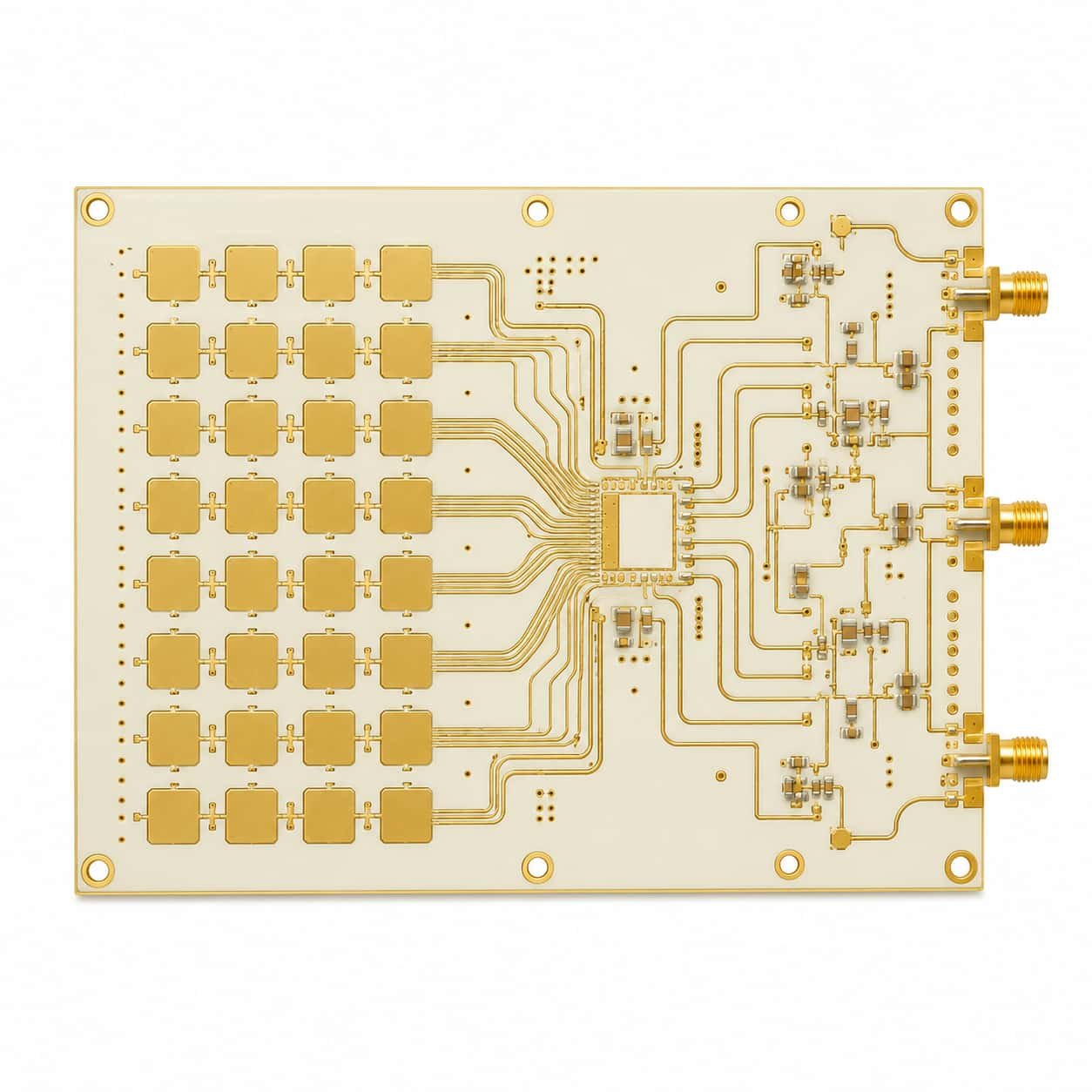
What Separates a Microwave PCB Manufacturer from a Standard PCB FactoryMicrowave PCB factory capability overview — Rogers materials, PTFE plasma activation, TDR verification
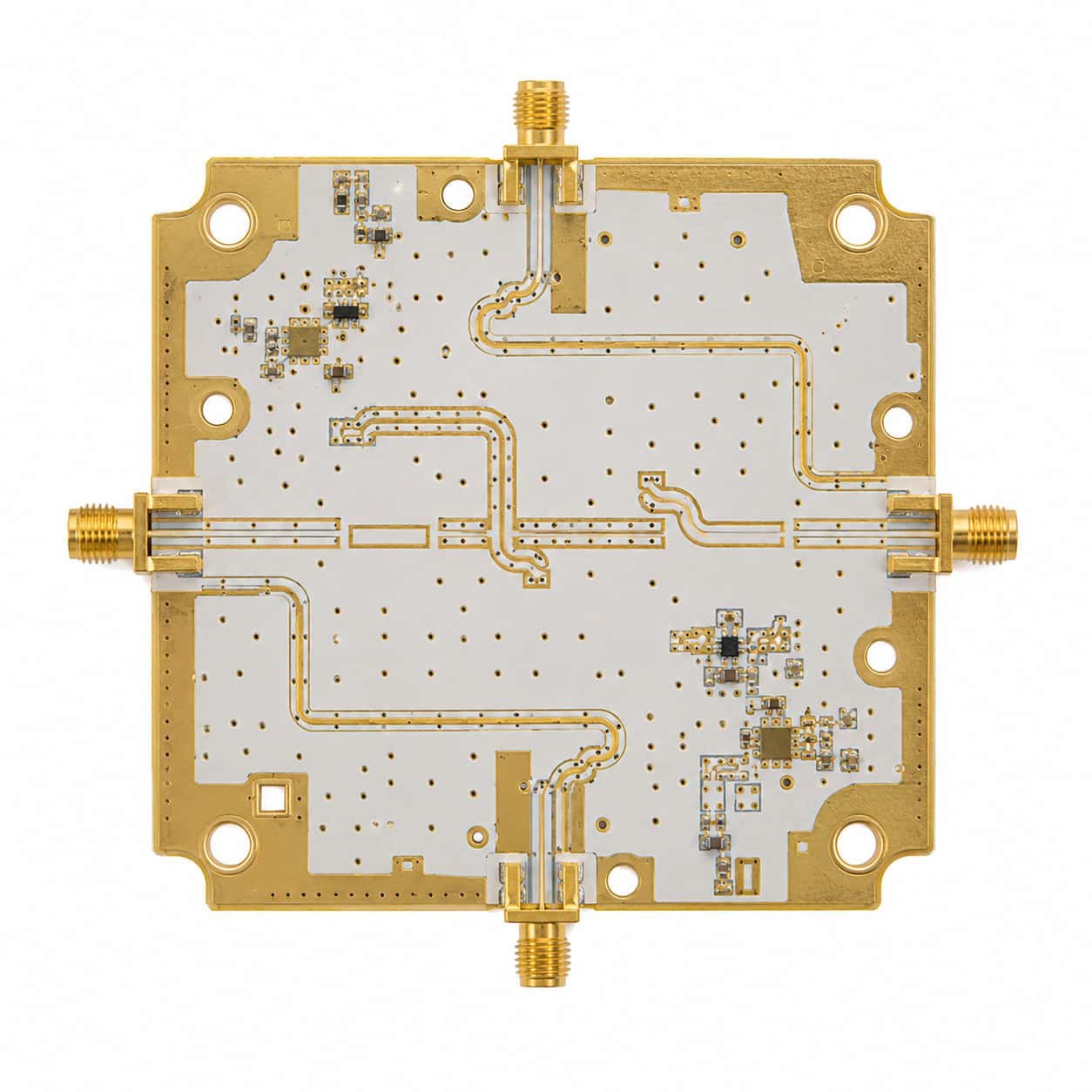
A standard FR4 PCB factory can process Rogers RO4350B (hydrocarbon ceramic) without any process modification — RO4350B uses the same drill parameters, press cycle, and plating process as FR4. This is why RO4350B is the most commonly available Rogers material at general PCB factories.

PTFE materials (Rogers RO3003, RT5880, Taconic TLY-5, F4B series) are completely different. They require:

  • In-house plasma or sodium naphthalene hole wall activation before copper plating — without this, copper deposits with zero adhesion
  • PTFE-specific drill parameters at reduced spindle speed to prevent smearing
  • Rogers 2929 bondply or equivalent for hybrid PTFE + FR4 stackups
  • Maximum 2 lamination press cycles — exceeding this causes PTFE deformation and Dk shift
  • TDR impedance verification on every production lot — not just first article

A factory that outsources plasma activation, uses standard FR4 drill parameters on PTFE, or only verifies impedance on first article samples is not a capable microwave PCB manufacturer — regardless of what its website states.

Materials Available at Riching PCB

Riching PCB stocks the following microwave PCB materials for same-week prototype:

Rogers Hydrocarbon Ceramic (FR4-compatible process)

  • RO4350B— Dk 3.48, Df 0.0037 — standard for 1–12 GHz
  • RO4003C — Dk 3.38, Df 0.0027 — lower loss for X-band and Ku-band

Rogers PTFE (plasma activation required)

  • RO3003 — Dk 3.0, Df 0.0010 — standard for Ka-band and 77 GHz radar
  • RT5880 — Dk 2.20, Df 0.0009 — lowest loss, wideband EW 2–18 GHz
  • RT5870 — Dk 2.33, Df 0.0012
  • RO3006 — Dk 6.15, Df 0.0020 — high Dk for compact antenna design
  • RO3010 — Dk 10.2, Df 0.0022
  • RO6010 — Dk 10.2, Df 0.0023

Taconic PTFE (plasma activation required)

  • TLY-5 — Dk 2.17, Df 0.0009
  • RF-35 — Dk 3.5, Df 0.0018
  • CER-10 — Dk 10.0, Df 0.0035

F4B PTFE Series

  • F4BM220 — Dk 2.20, Df 0.0010
  • F4BM255, F4BM265, F4BM300, F4B350 — Dk range 2.55–3.5

Full material thickness options available on the Rogers materials page and PTFE materials page.

Factory Capabilities

Capability Standard Available on Request
Materials RO4350B, RO4003C, RO3003, RT5880, Taconic, F4B Custom hybrid stackups
Frequency range DC to 77 GHz Above 77 GHz — consult
Layer count 2–16 layer Up to 36 layer
Min. line width 2.5 mil 2 mil with process review
Impedance tolerance ±10% ±5% with TDR verification
Min. drill diameter 0.2 mm mechanical 0.1 mm laser
PTFE plasma activation In-house, every order
Surface finish ENIG, immersion silver, OSP ENEPIG, hard gold
Board thickness 0.2–10 mm Custom
Prototype lead time 5–7 days (RO4350B) 7–10 days (PTFE)
MOQ No MOQ — from 1 board

Buyer Checklist: What to Verify Before Ordering

Verification Point What to Ask Why It Matters
PTFE plasma activation In-house or outsourced? Outsourced = process control risk
Rogers material stock Which grades and thicknesses in stock? Avoids long lead time on procurement
Impedance verification TDR on every lot or first article only? Every lot = consistent production
Copper foil type Standard ED or low-profile available? Critical above 20 GHz
IPC Class Class 2 or Class 3 certified? Class 3 required for aerospace/defense
DFM review Performed before every order? Catches stackup errors before fabrication
Lamination cycles Max press cycles for PTFE? Must be ≤2 for all PTFE materials

ApplicationsMicrowave PCB applications — radar, satellite, 5G and electronic warfare

  • Automotive radar — 24 GHz and 77 GHz FMCW radar front-end PCB
  • 5G infrastructure — base station RF front-end, massive MIMO antenna PCB
  • Satellite communication — Ku-band and Ka-band ground terminal PCB
  • Electronic warfare — wideband EW receiver and jammer PCB, 2–18 GHz
  • Aerospace radar — airborne weather radar, terrain avoidance PCB
  • Defense — phased array radar, missile guidance RF PCB
  • Industrial — microwave level measurement, process control radar

How to Get a Quote

Send the following to Riching PCB for DFM review and quotation within 24 hours:

  • Gerber files + NC drill file
  • Stackup drawing — material grade, dielectric thickness, copper weight per layer
  • Controlled impedance requirements and operating frequency
  • IPC Class (2 or 3) and quantity
  • Required lead time

Conclusion

A capable microwave PCB manufacturer must have in-house plasma activation for PTFE materials, Rogers and PTFE material stock, TDR impedance verification on every production lot, and a maximum of 2 lamination cycles for PTFE. Riching PCB is a direct factory in Shenzhen with full microwave PCB capability — Rogers RO4350B through RT5880 and RO3003, Taconic, and F4B in stock. See high frequency PCB capabilities for full specifications, or microwave PCB product page to place an order.

Get a Quote from a Direct Microwave PCB Factory

Rogers, PTFE, Taconic and F4B in stock. DFM review before every order. Send the following:

  • Gerber files + NC drill file
  • Stackup — material grade, dielectric thickness, copper weight per layer
  • Controlled impedance requirements and operating frequency
  • IPC Class and quantity
  • Required lead time

WhatsApp +86 13760473650 — quotation within 24 hours

Q&A

Microwave PCB Manufacturer Q&A

Common questions about microwave PCB manufacturing including material requirements, plasma activation, impedance verification, and lead times.

What materials does a microwave PCB manufacturer need to stock?

Rogers RO4350B (Dk 3.48, Df 0.0037) for RF up to 12 GHz; Rogers RO3003 (Df 0.0010, PTFE) and RT5880 (Df 0.0009, PTFE) for above 20 GHz; Taconic and F4B as cost-effective PTFE alternatives. All PTFE materials require in-house plasma hole wall activation.

What separates a microwave PCB manufacturer from a standard PCB factory?

In-house plasma activation for PTFE (standard factories outsource or skip), PTFE-specific drill parameters, maximum 2 lamination press cycles for PTFE, and TDR impedance verification on every production lot. Standard FR4 factories can process RO4350B without modification but cannot reliably manufacture PTFE microwave PCB.

Why must plasma activation be performed in-house?

Plasma activation must happen immediately before copper plating — any delay or contamination reduces effectiveness. Outsourcing introduces process control gaps that lead to copper adhesion failures on PTFE hole walls. Boards pass initial testing and fail in the field under thermal cycling.

What impedance tolerance should a microwave PCB manufacturer guarantee?

±10% standard, verified by TDR on every production lot. For above 20 GHz or antenna-critical designs, ±5% required. First-article-only verification is not sufficient — TDR must be performed on every lot to ensure consistent production quality.

What is the lead time for microwave PCB prototype?

RO4350B: 5–7 working days. RO3003 / RT5880 PTFE: 7–10 working days. No MOQ — from 1 board. DFM review before every order. WhatsApp: +86 13760473650.

PCB Project Review

Request a PCB Quote

Upload your Gerber ZIP file and project requirements. Our engineering team will review your PCB material, stackup, impedance needs, surface finish, and production quantity before quoting.

Please prepare:

  • Gerber files in ZIP format
  • PCB material or stackup requirements
  • Controlled impedance notes if available
  • Prototype or batch production quantity
ZIP format only. Please compress all Gerber and drill files into one ZIP package before uploading.