Rogers RO4350B PCB: Material Properties, Stackup Design and Manufacturing Guide

Table of Contents

Key point: Rogers RO4350B is a hydrocarbon ceramic laminate with Dk 3.48 and Df 0.0037. It processes on standard FR4-compatible equipment — no plasma activation required. Available thicknesses: 0.101, 0.168, 0.254, 0.338, 0.422, 0.508, 0.762, 1.524 mm. Standard for RF and microwave applications from 1 GHz to 12 GHz, including 5G sub-6GHz, WiFi 6, antenna systems, and radar front-ends. Riching PCB stocks RO4350B in all standard thicknesses. No MOQ. Prototype lead time 5–7 working days.

Rogers RO4350B is the most widely used high frequency PCB material in commercial RF and microwave design. It is a hydrocarbon ceramic laminate — not a PTFE material — which means it can be fabricated using standard FR4-compatible processes without plasma hole wall activation, special drill parameters, or PTFE bondply. This makes RO4350B the default choice for engineers who need reliable high frequency performance without the manufacturing complexity of pure PTFE substrates.

What Is Rogers RO4350B?

RO4350B belongs to the Rogers RO4000 series — a family of thermoset hydrocarbon ceramic laminates designed for RF and microwave PCB applications. The B suffix indicates the current production version with halogen-free flame retardant chemistry meeting UL 94 V-0.

Unlike PTFE-based Rogers materials (RO3003, RT5880), RO4350B does not require plasma hole wall activation before copper plating. It can be processed on the same equipment and press cycles as standard FR4, making it significantly easier and faster to fabricate — with no penalty on Dk stability or Df performance up to 12 GHz.

RO4350B Material Properties

Property Value Test Condition
Dielectric Constant (Dk) 3.48 ± 0.05 10 GHz, IPC-TM-650 2.5.5.5
Dissipation Factor (Df) 0.0037 10 GHz, IPC-TM-650 2.5.5.5
Thermal Coefficient of Dk (TCDk) +50 ppm/°C –50 to +150°C
CTE (x, y axis) 14 ppm/°C IPC-TM-650 2.4.41
CTE (z axis) 32 ppm/°C IPC-TM-650 2.4.41
Thermal Conductivity 0.69 W/m/K ASTM C518
Tg (Glass Transition) >280°C TMA
Flame Retardant UL 94 V-0

Available Thicknesses

RO4350B is available in the following standard dielectric thicknesses (not including copper foil):

0.101 mm / 0.168 mm / 0.254 mm / 0.338 mm / 0.422 mm / 0.508 mm / 0.762 mm / 1.524 mm

For controlled impedance designs, 0.254 mm and 0.508 mm are the most commonly used cores. Custom thicknesses are available on request.

RO4350B vs Other Rogers Materials

Material Dk Df Type Best For
RO4350B 3.48 0.0037 Hydrocarbon ceramic 1–12 GHz, 5G sub-6GHz, WiFi, antenna
RO4003C 3.38 0.0027 Hydrocarbon ceramic Lower loss than RO4350B, same process
RO3003 3.0 0.0010 PTFE ceramic Ka-band, 77 GHz, above 20 GHz
RT5880 2.20 0.0009 PTFE glass EW 2–18 GHz, wideband, lowest loss

RO4003C is the lower-loss alternative within the same hydrocarbon ceramic family — same FR4-compatible process, lower Df. See RO4003C vs RO4350B for a detailed comparison. For applications above 20 GHz, PTFE materials (RO3003, RT5880) are required.

Stackup Design for RO4350B4-layer hybrid PCB stackup diagram showing Rogers RO4350B outer dielectric layers, FR4 prepreg core, copper foil layers and top and bottom signal layers for high frequency PCB design

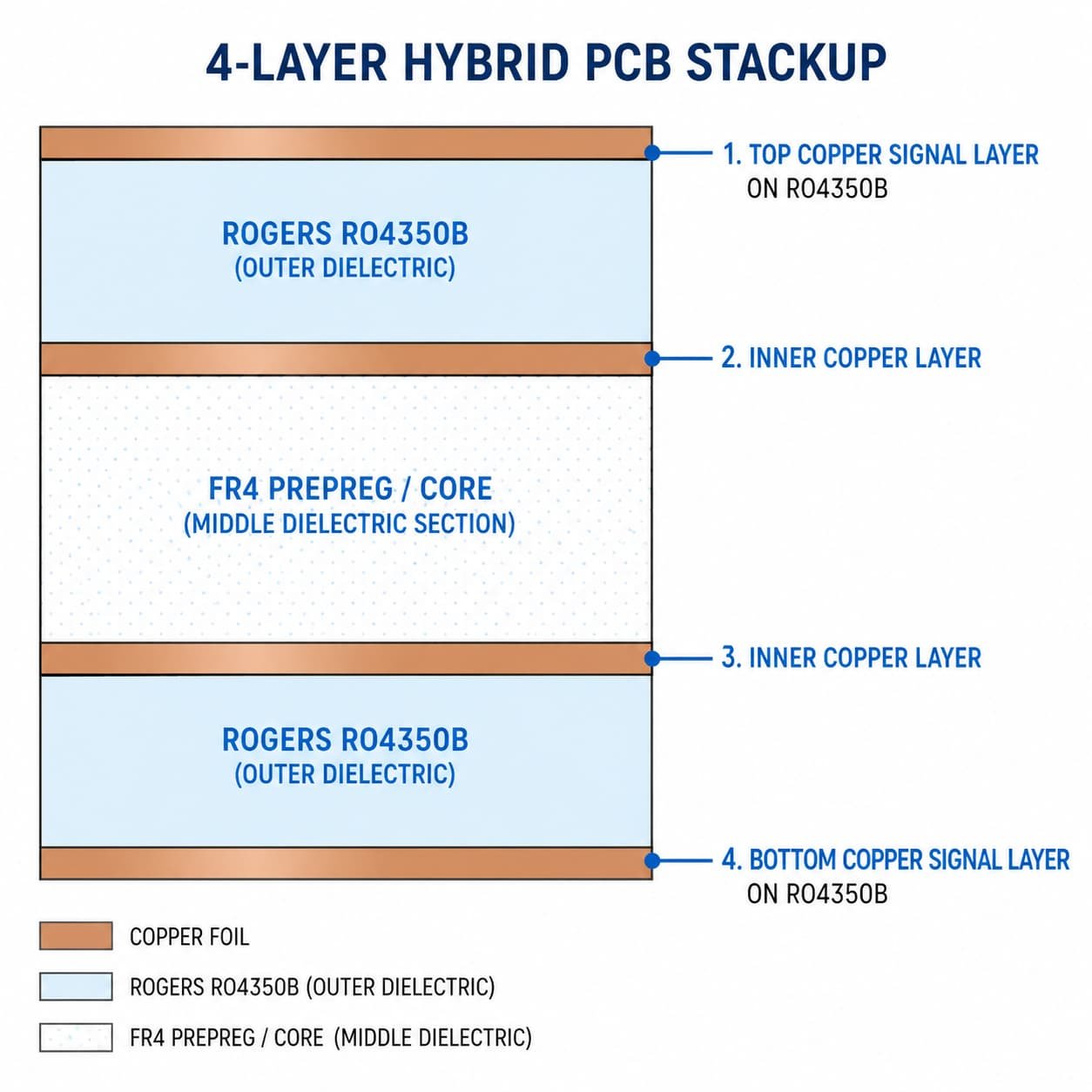
2-Layer RO4350B (most common for RF modules)

  • Top copper: 1 oz (35 µm) finished
  • RO4350B core: 0.254 mm or 0.508 mm
  • Bottom copper: 1 oz (35 µm) finished
  • Total board thickness: ~0.36 mm or ~0.62 mm


For 50Ω microstrip on 0.254 mm RO4350B with 1 oz copper: trace width approximately 0.56 mm. For 0.508 mm core: trace width approximately 1.14 mm. Confirm with your fabricator’s impedance calculator before finalizing layout.

4-Layer Hybrid Stackup (RO4350B + FR4)

  • L1 signal — RO4350B 0.254 mm core
  • L2 ground plane
  • FR4 prepreg
  • L3 power plane
  • FR4 prepreg
  • L4 signal — RO4350B 0.254 mm core


This stackup places RF signal layers on RO4350B while using FR4 for internal power and ground planes, reducing material cost significantly. See FR4 + Rogers hybrid PCB stackup guide for detailed design rules.

Manufacturing Requirements

Drilling

Standard mechanical drill parameters. No plasma activation required — key advantage over PTFE PCB materials. Minimum drill diameter 0.2 mm standard, 0.1 mm with laser.

Lamination

Standard FR4 press cycle compatible. For RO4350B + FR4 hybrid stackups, Rogers 4450F bondply is recommended as the prepreg between Rogers and FR4 layers.

Surface Finish

ENIG (immersion gold) is standard for RF applications. Immersion silver is acceptable for lower-cost prototypes. HASL is not recommended above 3 GHz due to surface flatness variation.

Controlled Impedance

±10% standard, ±5% available with TDR verification. Minimum line width 2.5 mil. Impedance tolerance must be specified on the fabrication drawing.

Copper Foil

Standard electrodeposited copper foil for most applications. For frequencies above 10 GHz, low-profile or reverse-treated copper foil reduces insertion loss from surface roughness.

ApplicationsHigh frequency RF PCB for 5G antenna application showing gold microstrip patch antenna array, RF feed traces and ENIG surface finish on Rogers RO4350B substrate

  • 5G sub-6GHz RF front-end modules and filters
  • WiFi 6 and WiFi 6E access point PCB
  • Antenna PCB for 2.4 GHz, 5 GHz, and 6 GHz
  • Radar front-end PCB at 24 GHz
  • Satellite communication ground equipment below 12 GHz
  • Power amplifier PCB for cellular base stations
  • FR4 + Rogers hybrid stackups for mixed RF/digital designs

Conclusion

RO4350B is the right choice for most RF and lower microwave applications below 12 GHz. Its combination of stable Dk, low Df, FR4-compatible processing, and broad thickness availability makes it the default starting point for Rogers PCB design. For applications above 20 GHz or where insertion loss budget is critical, evaluate RO4003C (same process, lower Df) or PTFE materials (RO3003, RT5880).

Order RO4350B PCB from a Direct Factory

Riching PCB stocks Rogers RO4350B in all standard thicknesses. Send the following for DFM review and quotation:

  • Gerber files + NC drill file
  • RO4350B core thickness and copper weight per layer
  • Stackup drawing — single material or FR4 hybrid
  • Controlled impedance requirements
  • Quantity and required lead time

WhatsApp +86 13760473650 — prototype lead time 5–7 working days

PCB Project Review

Request a PCB Quote

Upload your Gerber ZIP file and project requirements. Our engineering team will review your PCB material, stackup, impedance needs, surface finish, and production quantity before quoting.

Please prepare:

  • Gerber files in ZIP format
  • PCB material or stackup requirements
  • Controlled impedance notes if available
  • Prototype or batch production quantity
ZIP format only. Please compress all Gerber and drill files into one ZIP package before uploading.