
RF and Digital Mixed-Signal PCB Stackup Design: Isolation Rules for Tunable Filter MMIC Evaluation Boards (20MHz–26GHz)
Digitally tunable RF filters and switched-filter-bank MMICs are increasingly used to cover wide instantaneous bandwidths — from tens of MHz up into the mid-20GHz range — inside a single component. This class of device replaces banks of discrete filters and switches, tunes in well under a microsecond, and typically offers 40-50dB of out-of-band rejection with power handling around the +20 to +25dBm range. The applications sit squarely inside AESA radar front ends, electronic warfare receivers, SIGINT systems, software-defined radios, spectrum monitoring equipment, and aerospace communication links. For a board house, the interesting part is not the MMIC itself — it's what the MMIC does to the layout. Folding a filter bank into one packaged part removes discrete component count, but it concentrates the RF path, the DC bias, and a digital control bus onto the same small evaluation board. That combination is where most first-pass boards fail electrical test, not because the material was wrong, but because the RF and digital domains were not properly separated in the stackup.
Home » RF and Digital Mixed-Signal PCB Stackup Design for Tunable Filter MMIC Evaluation Boards
Table of Contents
Why This Is a Stackup Problem, Not Just a Layout Problem
A tunable or switched-filter MMIC evaluation board has to carry two very different kinds of signal on the same substrate: a continuous RF path that needs a clean, low-loss, well-referenced transmission line from input connector to output connector, and a parallel or serial digital control bus that sets the tuning state. The control bus is DC-to-low-frequency by function, but its edges are fast — sub-200ns switching produces broadband harmonic content that overlaps directly with the RF passband. If the RF and digital sections share a return path, or if the digital layer sits too close to the RF layer without its own reference plane, switching transients couple straight into the signal chain as spurious tones or an elevated noise floor.
This is a stackup decision because it has to be resolved in layer assignment and plane placement before routing starts — it cannot be fixed afterward by re-routing a few traces.
Stack-up Allocation for RF and Digital Domains
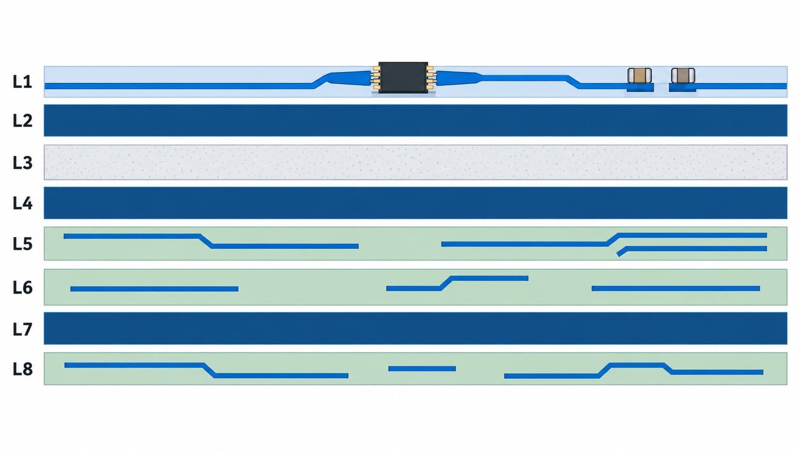
A working approach separates the board into a dedicated RF zone and a dedicated digital/control zone, each with its own uninterrupted ground reference:
- A top RF layer on a low-loss laminate, with a solid ground plane directly beneath it and no digital traces routed on that plane.
- At least one full ground layer isolating the RF layer from any digital or DC-bias routing layers below it.
- Digital control and bias distribution kept on lower layers, referenced to their own ground, with minimal via transitions back up toward the RF zone.
- A transition to standard FR-4 core layers for the mechanical body of the board, bonded to the RF laminate only where the RF layer requires it.
| Layer | Function | Reference Plane | Typical Laminate | Notes |
|---|---|---|---|---|
| L1 (Top) | RF signal — MMIC RF I/O, 50Ω microstrip | L2, solid GND directly beneath | Low-loss hydrocarbon-ceramic RF laminate | Via-fenced; no digital traces on this layer |
| L2 | Ground — RF reference plane | — | Same RF laminate, bonded to L1 | Continuous pour, stitched to L1 via fence |
| L3 | Isolation ground | — | FR-4 core (bonding layer) | Separates RF zone from digital zone below; full pour, no breaks |
| L4 | Digital control routing (SPI / parallel tuning bus) | L5, digital GND | Standard FR-4 | Cross RF traces at 90° only; never route parallel to L1 |
| L5 | Ground — digital reference plane | — | Standard FR-4 | Continuous pour under digital routing |
| L6 | DC bias distribution | L5 / L7 | Standard FR-4 | Decoupling caps at MMIC pins, not routed on this layer alone |
| L7 | Ground / thermal plane | — | Standard FR-4 | Stitched to L2 & L5; supports thermal relief under MMIC |
| L8 (Bottom) | Mechanical / secondary routing, test points | L7 | Standard FR-4 | Optional coupon routing, connector mounting pads |
This kind of hybrid construction is the same principle used on Rogers/FR-4 hybrid stack-ups, adapted here specifically for a board that also has to route a digital control bus without letting it interfere with the RF section.
Ground Via Fencing and RF Compartmentalization
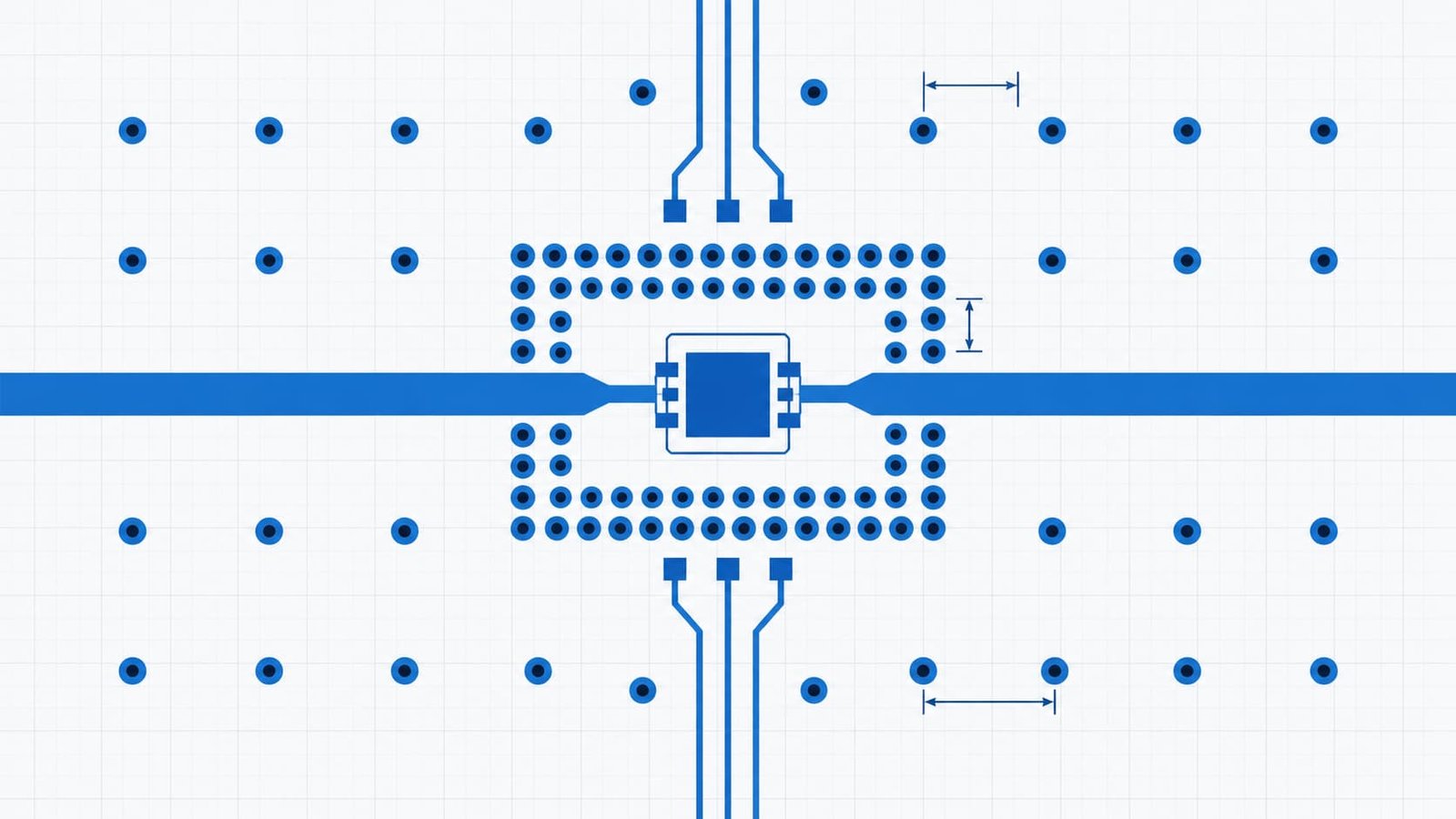
Once the layers are assigned, the RF trace and the MMIC footprint need to be physically compartmentalized with stitching vias. A continuous fence of ground vias around the RF trace and the filter package, tied through to the ground layer beneath, keeps the RF energy from radiating sideways into the digital zone and keeps digital return current from crossing under the RF trace. Via pitch should stay well below the guard-band needed at the highest operating frequency in the band — as the operating frequency pushes toward 26GHz, the fence needs to be noticeably tighter than what is acceptable on a lower-frequency board, or it stops acting as a continuous wall and starts leaking.
The same fencing discipline should extend to the shield-can or cavity contact points if the evaluation board uses a metal lid — inconsistent ground contact around the lid perimeter reintroduces the same leakage the via fence was built to prevent.
Digital Control Line Isolation and Decoupling
Every control and bias pin on the MMIC package is a potential entry point for RF energy to leak out, or for digital switching noise to leak in. A few rules keep that risk manageable:
- Place decoupling capacitors directly at the MMIC bias and control pins, not routed back to a shared plane several millimeters away.
- Add low-pass filtering — typically a ferrite bead or small series resistor with a shunt capacitor — on control lines at the point where they cross from the digital zone into the RF compartment.
- Route control traces perpendicular to RF traces where a crossing is unavoidable, and never run them in parallel for any meaningful length.
- Keep the digital driver and any clock or SPI-type signal physically as far from the RF connector launches as the board outline allows.
If RF/digital isolation is treated as a routing afterthought rather than a stackup decision, the symptoms usually don’t show up until full-power or production test — unstable tuning states, spurious tones tied to the control clock, or an elevated noise floor that wasn’t visible on a bare S-parameter sweep. At that stage a respin is far more expensive than getting the layer assignment right before layout starts. |
Broadband 50Ω Transitions and Connector Launch
A filter that tunes across a wide band is only as good as the transitions on either side of it. The connector launch and the microstrip-to-package transition into the MMIC both need to hold a controlled 50Ω impedance across the full tuning range, not just at a single design frequency. At the upper end of a 20MHz-26GHz range, footprint parasitics at the MMIC package pads start to matter as much as the transmission line geometry itself, and copper roughness on the RF layer becomes a measurable contributor to insertion loss.
Material Notes
Hydrocarbon-ceramic laminates are a common choice for boards in this frequency range because they balance low loss with standard multilayer processing, which keeps hybrid RF/digital builds manufacturable at reasonable cost. Where an application specifically prioritizes the lowest possible insertion loss over ease of processing, PTFE-based laminates are the alternative worth evaluating on their own electrical merits. The right choice depends on the specific loss budget, layer count, and production volume of the board — it’s a selection decision based on the application, not a one-for-one substitution between material families.
Validating the Build: Coupons and VNA Data
For a board like this, a statement of “we can build Rogers boards” is not enough evidence for a customer qualifying a new supplier. What matters is de-embedded test coupon data across the full 20MHz-26GHz range — insertion loss, return loss, and isolation between the RF and digital compartments — delivered alongside the boards, plus a connector launch that has actually been tuned and measured rather than just simulated.
This connects directly to RF test fixture design and to the grounding and shielding practices covered in the LNA grounding and shielding guide — both are the same underlying discipline applied to a different part of the RF chain.
What to Look for in a Manufacturing Partner
A tunable-filter MMIC evaluation board sits at the intersection of a few capability areas that not every fabricator carries at the same time:
- Experience building hybrid RF/FR-4 stackups, not just single-material RF boards.
- Via fencing and ground stitching executed to the tolerances the frequency actually requires, not a generic default.
- Connector launch tuning backed by measured VNA data, not simulation alone.
- Familiarity with the export-control and end-use screening questions that come with radar, EW, and defense-adjacent programs.
These same fundamentals carry over from related builds such as phased array antenna PCBs and automotive radar PCBs, where RF/digital coexistence on one board is just as central to getting a working first article.
RF Digital Mixed-Signal PCB Stackup — Q&A
Common questions on isolating RF and digital control domains on tunable filter MMIC evaluation boards.
What frequency range needs RF/digital isolation on a mixed-signal PCB?
Isolation matters most as frequency climbs into the GHz range. On a 20MHz-26GHz tunable filter MMIC board, sub-200ns switching edges generate broadband noise that overlaps the RF passband, so layer separation and via fencing are needed even though the control bus itself is low frequency.
How many ground vias are needed to fence an RF section?
There's no single fixed count — the via pitch has to stay small relative to the shortest wavelength in the tuning range so the fence acts as a continuous wall, not a row of gaps. Near 26GHz that pitch needs to be noticeably tighter than on a lower-frequency board.
Can standard FR-4 be used for a 26GHz tunable filter MMIC board?
Not for the RF signal layer alone — FR-4's dielectric loss is too high at these frequencies. A hybrid stackup pairing a low-loss RF laminate with FR-4 core layers for the digital and mechanical body is the more practical approach.
Why does switching noise matter if the control lines are DC/low frequency?
A fast logic edge isn't one frequency — it's a spectrum of harmonics reaching well above the switching rate. Sub-200ns transitions can generate harmonics that land directly inside a 20MHz-26GHz passband if the control lines aren't filtered and kept isolated from the RF zone.
Need an RF/Digital Hybrid Stackup for Your Filter MMIC Board?
We build hybrid RF/FR-4 stackups for tunable filter MMIC evaluation boards, radar front ends, and EW receivers — with via-fenced RF compartments and de-embedded VNA coupon data delivered on every build.
Get a Quote → WhatsAppRequest a PCB Quote
Upload your Gerber ZIP file and project requirements. Our engineering team will review your PCB material, stackup, impedance needs, surface finish, and production quantity before quoting.
Please prepare:
- Gerber files in ZIP format
- PCB material or stackup requirements
- Controlled impedance notes if available
- Prototype or batch production quantity