
Ordering an RF PCB prototype from China offers 40–60% cost savings vs Western fabricators with comparable technical capability — provided you order from a direct factory rather than a trading company, and you know what information to provide upfront. Missing or incomplete information at order time is the most common cause of delays, not the factory’s manufacturing process.
This guide covers exactly what files to send, how DFM review works, lead times for different Rogers and PTFE materials, the door-to-door timeline from Shenzhen to Europe and North America, and what to check when boards arrive.
Lead Times for RF PCB Prototype from China
Rogers RO4350B and RO4003C — 5–7 Working Days
RO4350B and RO4003C are hydrocarbon ceramic laminates that process on standard FR4-compatible equipment. No plasma activation required. Material is in stock at Riching PCB in all standard thicknesses. Lead time is 5–7 working days from DFM confirmation to ship — not from order placement.
Rogers RO3003, RT5880 and Other PTFE — 7–10 Working Days
All PTFE materials require in-house plasma hole wall activation before copper plating. This adds 1–2 days to the process sequence. Lead time is 7–10 working days from DFM confirmation to ship. Note: a factory quoting 5–7 days for RO3003 is either not performing plasma activation or has misunderstood the order — both produce defective boards. See PTFE PCB manufacturing guide for why plasma activation cannot be skipped.
Rogers + FR4 Hybrid Stackup — 10–14 Working Days
Hybrid stackups require DFM review of the bondply selection, press cycle planning, and registration requirements before fabrication starts. Allow 10–14 working days for hybrid prototype. DFM review is mandatory — do not place a hybrid stackup order without confirming the stackup with the factory first.
Door-to-Door Timeline: China to Europe / North America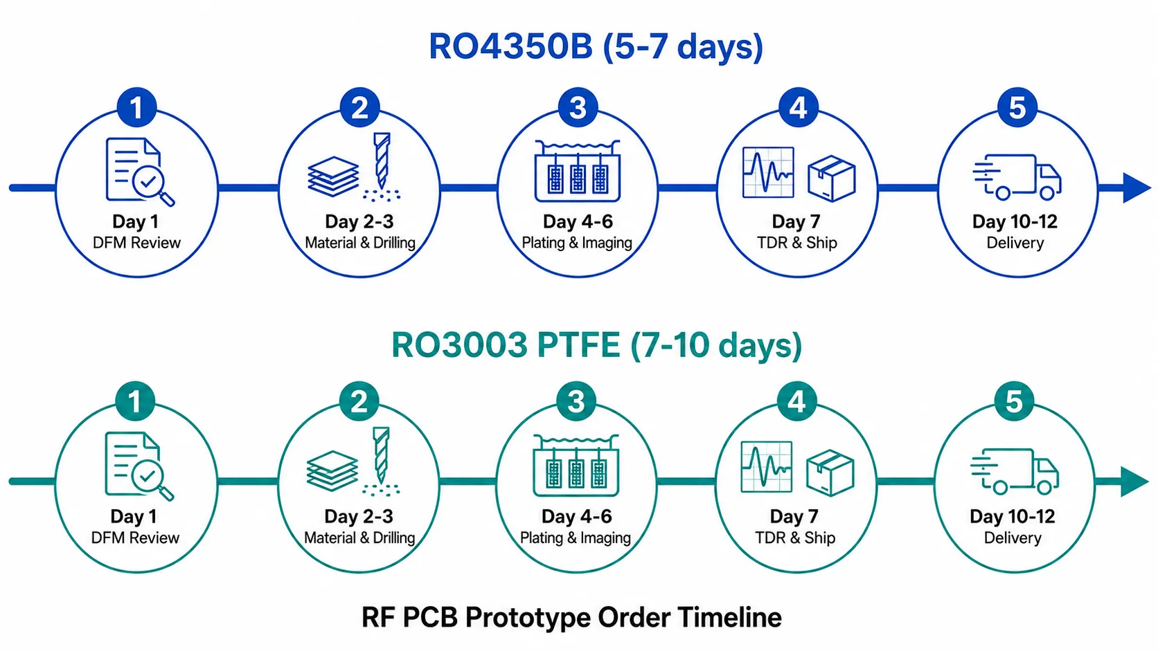
The Stackup Drawing — Most Common Missing Item
Rogers PCB cannot be quoted or fabricated without a stackup drawing. The Gerber files do not contain material grade, dielectric thickness, or copper weight per layer. At minimum, provide: Rogers material grade (e.g. RO4350B), dielectric thickness (e.g. 0.508 mm), copper weight per layer (e.g. 1 oz outer, 0.5 oz inner), and total board thickness target. A hand-drawn or text-described stackup is acceptable for prototype — the factory will formalize it during DFM review.
How DFM Review Works
Every RF PCB prototype order at Riching PCB goes through DFM (Design for Manufacturability) review before fabrication starts. This is not a formality — DFM review catches design issues that cause prototype failures or production delays.
DFM review covers:
- Line width and spacing vs copper weight — confirms minimum feature sizes are achievable
- Annular ring size vs drill diameter — confirms via reliability
- Controlled impedance trace width vs stackup Dk — confirms the impedance calculation matches the stackup
- Via aspect ratio vs board thickness — confirms plating capability
- PTFE-specific checks — bondply selection, maximum lamination cycles, plasma activation requirement
- Hybrid stackup checks — Rogers/FR4 interface, press cycle count, bondply compatibility
DFM review typically completes within 4–8 hours on business days (GMT+8). If issues are found, engineering contacts you before fabrication starts — not after. This prevents costly re-spins from avoidable design errors.
Why Order RF PCB Prototype from China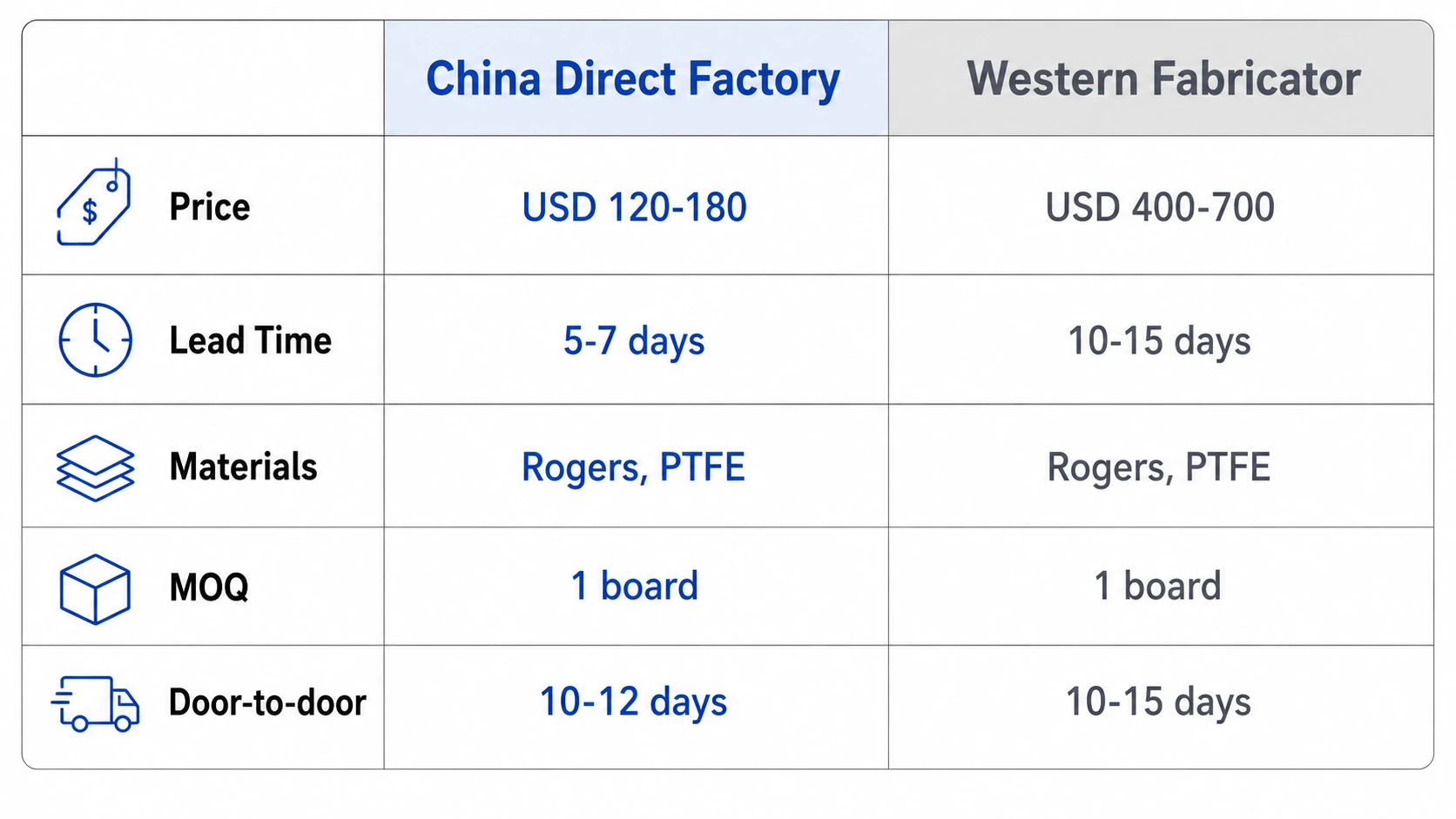
Cost — 40–60% Lower
A Rogers RO4350B 2-layer prototype (100×100mm, 10 boards) costs approximately USD 120–180 from Riching PCB, compared to USD 400–700 from a US or European fabricator. See Rogers PCB price guide for detailed cost comparison by board spec.
Lead Time — Comparable or Faster
5–7 working days for RO4350B plus 3–5 days DHL shipping = 10–12 days door-to-door. Many Western fabricators quote 10–15 days manufacturing lead time alone, before shipping. For PTFE materials, Chinese factory + DHL is typically faster total than a Western fabricator’s manufacturing lead time.
Technical Capability — Equivalent
A capable Chinese Rogers PCB factory uses the same Rogers materials, the same IPC standards, and the same TDR verification as Western fabricators. The key is choosing a factory with genuine in-house PTFE plasma activation capability. See how to verify China PTFE PCB manufacturer capability for the verification checklist.
What to Check When Boards Arrive
- Visual inspection: solder mask coverage, ENIG finish uniformity, board outline dimensions
- Dimensional check: board size vs drawing, drill diameter spot check
- TDR report: request the impedance measurement report if not included in the shipment — Riching PCB provides this on request for every lot
- Material certificate: Rogers material lot certificate available on request — confirms actual Dk of the material used
- First power-on: check continuity and isolation before mounting components
How to Place an Order
- Send Gerber files + NC drill file + stackup drawing via WhatsApp or email
- Specify: Rogers material grade and thickness, copper weight, controlled impedance requirements, IPC Class, surface finish, quantity, delivery address
- DFM review completed within 4–8 hours — engineering confirms stackup and impedance before fabrication
- Confirm order — fabrication starts same day for RO4350B, next day for PTFE
- Boards shipped via DHL Express with tracking — delivery confirmation sent on ship day
Conclusion
RF PCB prototype from China: RO4350B 5–7 working days, PTFE materials 7–10 working days, door-to-door to Europe and North America 10–15 days total. No minimum order quantity. DFM review on every order before fabrication starts. The most important preparation is the stackup drawing — material grade, thickness, copper weight per layer, and controlled impedance requirements. Riching PCB is a direct factory in Shenzhen with full Rogers and PTFE capability. See high frequency PCB capabilities for full factory specifications.