Rogers PCB Prototype: Lead Time, File Requirements and How to Order
Everything you need to prepare before ordering a Rogers PCB prototype — file checklist, material specification, lead times for RO4350B and PTFE materials, and what to expect from DFM review.
Home » High Frequency PCB Prototype » Rogers PCB Prototype: Lead Time, File Requirements and How to Order
Table of Contents
Key point: Rogers RO4350B and RO4003C prototype lead time is 5–7 working days — FR4-compatible process. Rogers RO3003 and RT5880 PTFE prototype is 7–10 working days — plasma activation adds 1–2 days. The most important preparation step is the stackup drawing: material grade, dielectric thickness, copper weight per layer, and controlled impedance requirements. Without a complete stackup drawing, DFM review cannot start. Riching PCB performs DFM review on every prototype order before fabrication. No MOQ — from 1 board.
Ordering a Rogers PCB prototype for the first time involves more preparation than a standard FR4 order. The fabricator needs more information upfront — material grade, dielectric thickness, copper weight per layer, controlled impedance requirements, and IPC Class — because these parameters directly affect the manufacturing process and cannot be assumed from the Gerber files alone.
This guide covers exactly what files to prepare, what to specify on the order, how lead time differs between Rogers RO4350B and PTFE materials, what DFM review covers, and what to expect from Riching PCB on every prototype order.
Rogers PCB Prototype Lead Times
| Material | Process Type | Prototype Lead Time | Notes |
|---|---|---|---|
| RO4350B | FR4-compatible | 5–7 working days | All standard thicknesses in stock |
| RO4003C | FR4-compatible | 5–7 working days | All standard thicknesses in stock |
| RO3003 | PTFE — plasma required | 7–10 working days | 0.127 mm and 0.254 mm in stock |
| RT5880 | PTFE — plasma required | 7–10 working days | 0.127–3.175 mm in stock |
| Taconic TLY-5 / RF-35 | PTFE — plasma required | 7–10 working days | In stock |
| F4BM220 / F4B series | PTFE — plasma required | 7–10 working days | In stock |
| Rogers + FR4 hybrid | 2 press cycles max | 10–14 working days | DFM review required before start |
The key distinction is RO4350B/RO4003C (hydrocarbon ceramic, FR4-compatible process) vs PTFE materials (RO3003, RT5880, Taconic, F4B). PTFE adds 2–3 days due to plasma hole wall activation — a mandatory process step that cannot be shortened.
What Files to Prepare
| File / Information | Required | Notes |
|---|---|---|
| Gerber files (all copper layers) | ✅ Required | RS-274X format preferred |
| Solder mask layers (top + bottom) | ✅ Required | Both sides |
| Board outline (mechanical layer) | ✅ Required | Single closed outline |
| NC drill file | ✅ Required | Excellon format, all drill sizes |
| Stackup drawing | ✅ Required | Material grade, thickness, copper weight per layer |
| Controlled impedance notes | If applicable | Target impedance, tolerance, reference layer |
| Rogers material grade + thickness | ✅ Required | e.g. RO4350B 0.254 mm, 1 oz copper |
| IPC Class (2 or 3) | Recommended | Default Class 2 if not specified |
| Surface finish | Recommended | Default ENIG if not specified |
| Quantity and delivery address | ✅ Required | For quotation and shipping calculation |
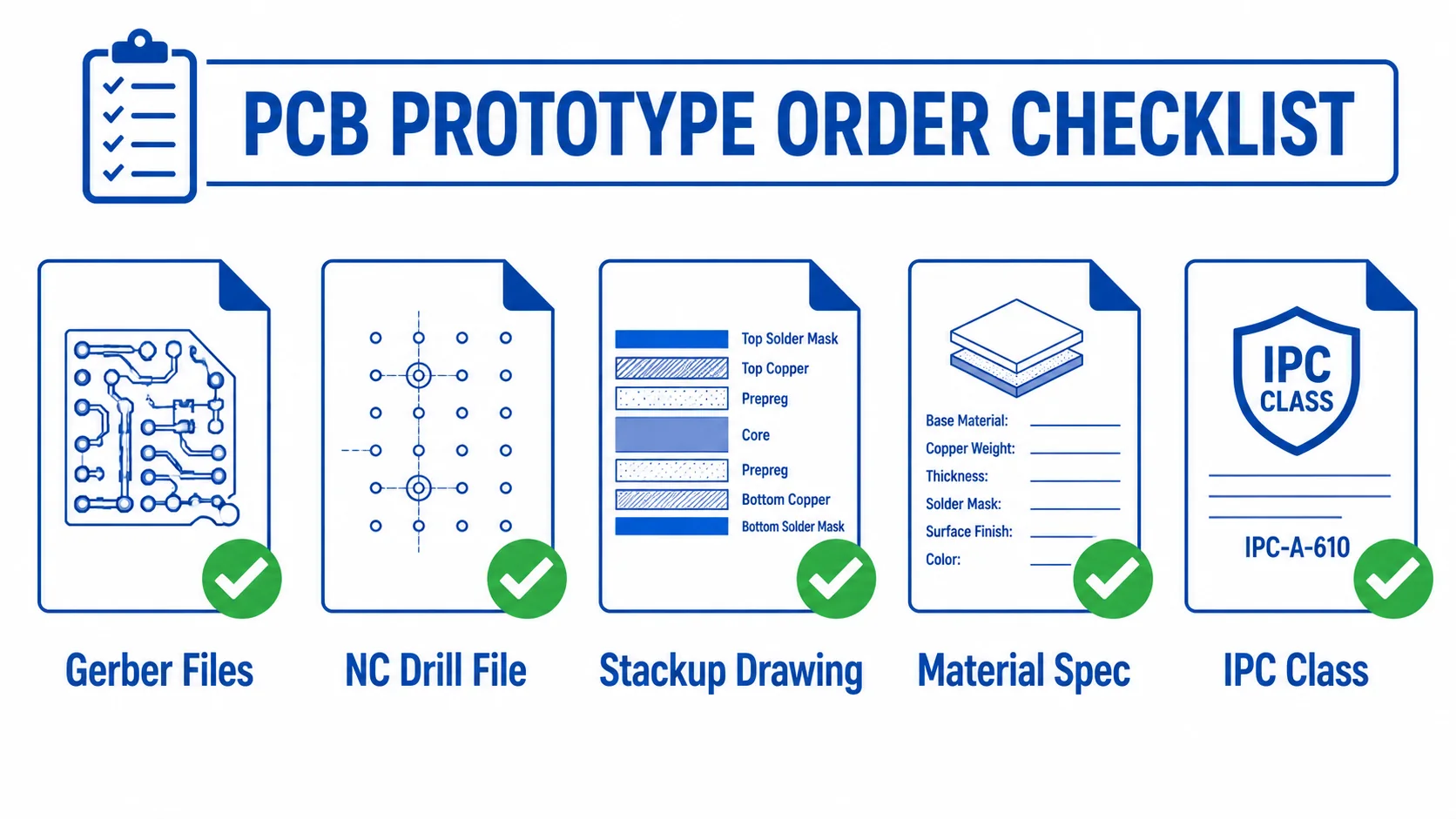
The Stackup Drawing — Most Commonly Missing
The most common reason for prototype delays is a missing or incomplete stackup drawing. For Rogers PCB, the fabricator cannot assume material thickness, copper weight, or dielectric constant from the Gerber files. The stackup drawing must specify:
- Layer sequence (L1 signal, L2 ground, L3 power, L4 signal, etc.)
- Material grade for each dielectric layer (e.g. RO4350B 0.254 mm core, Rogers 4450F prepreg)
- Copper weight for each layer (e.g. 0.5 oz, 1 oz, 2 oz)
- Total finished board thickness target
- Controlled impedance requirements (trace width, target impedance, reference layer, tolerance)
If you do not have a formal stackup drawing, a clear written specification in the order notes is acceptable for prototype. Riching PCB engineering will confirm the stackup before fabrication starts.
What Happens After You Send Files
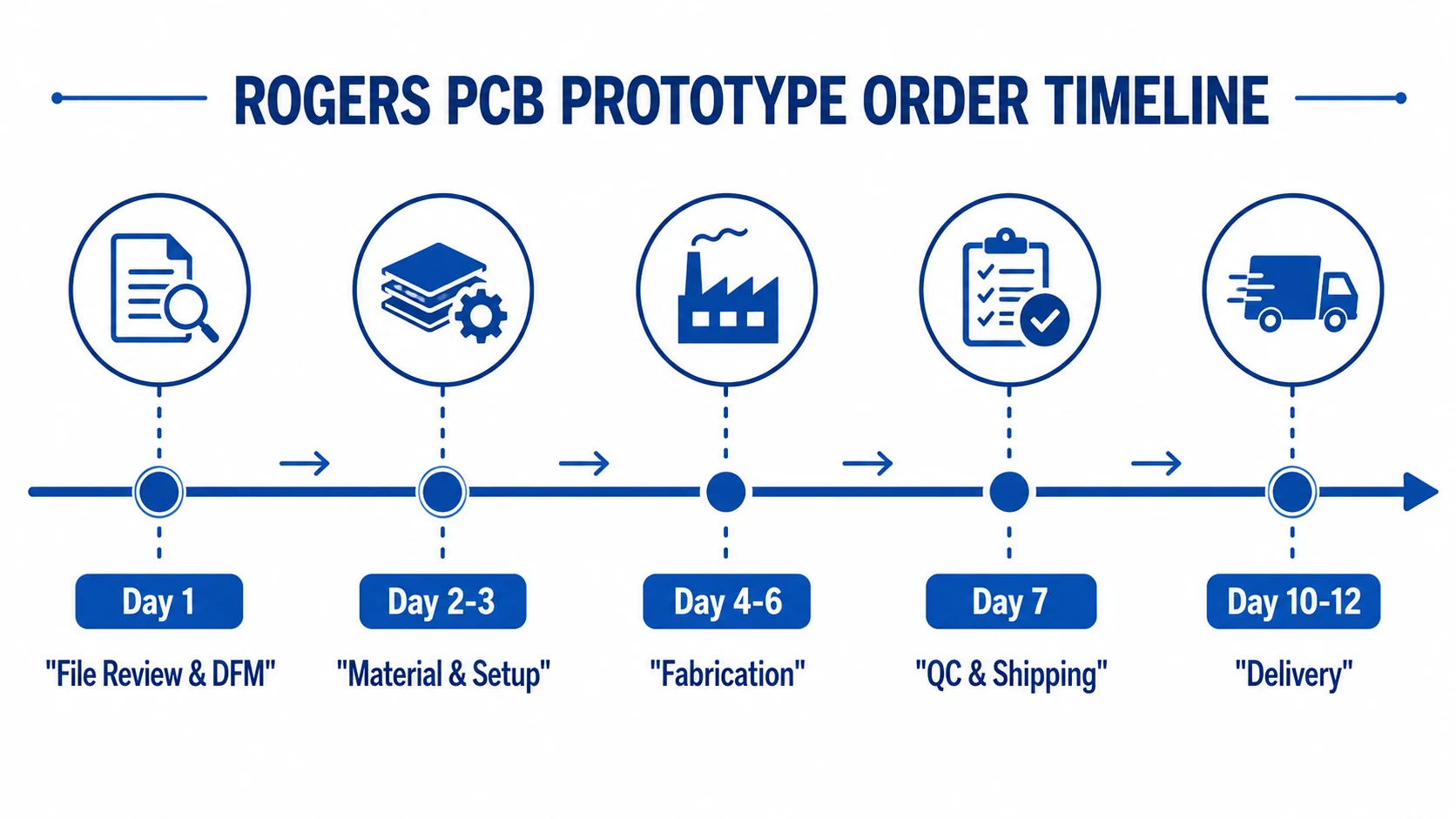
DFM Review (Day 1)
Every Rogers PCB prototype order at Riching PCB goes through DFM (Design for Manufacturability) review before fabrication starts. DFM review checks: minimum line width and spacing vs copper weight, annular ring size vs drill diameter, controlled impedance trace width vs stackup, via aspect ratio vs board thickness, and PTFE-specific constraints (lamination cycles, bondply selection for hybrid stackups).
DFM review typically completes within 4–8 hours. If issues are found, engineering contacts you with specific questions before fabrication — not after. This prevents costly re-spins from avoidable errors.
Material and Process Setup (Day 2–3)
For RO4350B and RO4003C, material is cut from stock and inner layer imaging begins on Day 2. For PTFE materials (RO3003, RT5880), plasma activation is performed on the drilled board before copper plating — this adds approximately 1 working day to the process sequence.
Fabrication and Impedance Verification
Controlled impedance is verified by TDR (Time Domain Reflectometry) on test coupons in the panel. For ±10% tolerance (standard), TDR is performed on the production panel. For ±5% tolerance, request this explicitly on the order — it is available at additional lead time. See controlled impedance RF PCB guide for detailed TDR specification guidance.
Common Rogers PCB Prototype Mistakes
Specifying Material Grade Without Thickness
‘Rogers RO4350B’ is not a complete material specification. The fabricator needs the dielectric thickness — 0.101, 0.168, 0.254, 0.338, 0.422, 0.508, or 0.762 mm. Different thicknesses produce different 50Ω trace widths. If thickness is not specified, the fabricator will ask — adding a day to the order.
Using FR4 Copper Weights on PTFE
Standard FR4 prototype orders often use 1 oz outer copper. For Ka-band and mmWave PTFE designs, 0.5 oz outer copper reduces surface roughness contribution to insertion loss. Specify copper weight per layer explicitly on the stackup drawing.
Not Specifying Impedance Tolerance
If controlled impedance is required, specify the tolerance (±10% or ±5%) on the fabrication drawing. Without a specified tolerance, the fabricator applies the standard ±10%. For phased array and mmWave designs requiring ±5%, this must be stated explicitly.
Assuming Rogers + FR4 Hybrid Is Standard Lead Time
Rogers RO4350B + FR4 hybrid stackups require Rogers 4450F bondply and a specific press cycle — lead time is 10–14 working days, not 5–7. Plan accordingly. See FR4 + Rogers hybrid PCB stackup guide for full design requirements.
How to Order
- Send Gerber files, NC drill file, and stackup drawing to WhatsApp +86 13760473650 or email
- Include material grade, dielectric thickness, copper weight per layer, and controlled impedance requirements
- Specify IPC Class (default Class 2) and surface finish (default ENIG)
- DFM review and quotation returned within 4–8 hours on business days
- Confirm order — fabrication starts same day for RO4350B, next day for PTFE
Conclusion
Rogers PCB prototype lead time at Riching PCB: RO4350B and RO4003C 5–7 working days, PTFE materials 7–10 working days. No minimum order quantity. The most important preparation step is the stackup drawing — material grade, dielectric thickness, copper weight per layer, and controlled impedance requirements. DFM review is performed on every order before fabrication starts. See Rogers materials page for available thicknesses, or contact via WhatsApp for a same-day quotation.
Order Your Rogers PCB Prototype
No MOQ. DFM review before every order. Send the following to start:
- Gerber files + NC drill file
- Stackup drawing — Rogers material grade, dielectric thickness, copper weight per layer
- Controlled impedance requirements (if applicable)
- IPC Class and surface finish
- Quantity and delivery address
WhatsApp +86 13760473650 — DFM review and quotation within 4–8 hours
Rogers PCB Prototype Q&A
Common questions about Rogers PCB prototype lead times, file requirements, DFM review and minimum order quantity.
What is the lead time for Rogers PCB prototype?
RO4350B and RO4003C: 5–7 working days. RO3003 and RT5880 PTFE: 7–10 working days — plasma activation adds 1–2 days. Rogers + FR4 hybrid: 10–14 working days. No MOQ — from 1 board.
What files do I need to send for a Rogers PCB prototype?
Required: Gerber files (all layers, solder mask, outline), NC drill file, stackup drawing (Rogers material grade, dielectric thickness, copper weight per layer). Also specify: controlled impedance requirements, IPC Class (default 2), surface finish (default ENIG), quantity, delivery address. Stackup drawing is the most commonly missing item.
What does DFM review cover for Rogers PCB prototype?
Line width/spacing vs copper weight, annular ring vs drill, impedance trace width vs stackup Dk, via aspect ratio, PTFE lamination limits and bondply selection. Completes within 4–8 hours. Issues flagged before fabrication starts — not after.
Can I order 1 Rogers PCB prototype board?
Yes — no MOQ, from 1 board. RO4350B, RO4003C, RO3003, RT5880, Taconic and F4B all in stock. DFM review on every order regardless of quantity.
Why is a stackup drawing required for Rogers PCB prototype?
Gerber files do not contain material thickness, copper weight, or Dk. Different RO4350B thicknesses produce different 50Ω trace widths. Without stackup drawing, DFM review cannot confirm the impedance calculation or fabrication process.
Request a PCB Quote
Upload your Gerber ZIP file and project requirements. Our engineering team will review your PCB material, stackup, impedance needs, surface finish, and production quantity before quoting.
Please prepare:
- Gerber files in ZIP format
- PCB material or stackup requirements
- Controlled impedance notes if available
- Prototype or batch production quantity
